AT90S4414/8515
65
•
INT1 - Port D, Bit 3
INT1, External Interrupt source 1: The PD3 pin can serve as an external interrupt source to the MCU. See the interrupt
description for further details, and how to enable the source.
•
INT0 - Port D, Bit 2
INT0, External Interrupt source 0: The PD2 pin can serve as an external interrupt source to the MCU. See the interrupt
description for further details, and how to enable the source.
•
TXD - Port D, Bit 1
Transmit Data (Data output pin for the UART). When the UART transmitter is enabled, this pin is configured as an output
regardless of the value of DDRD1.
•
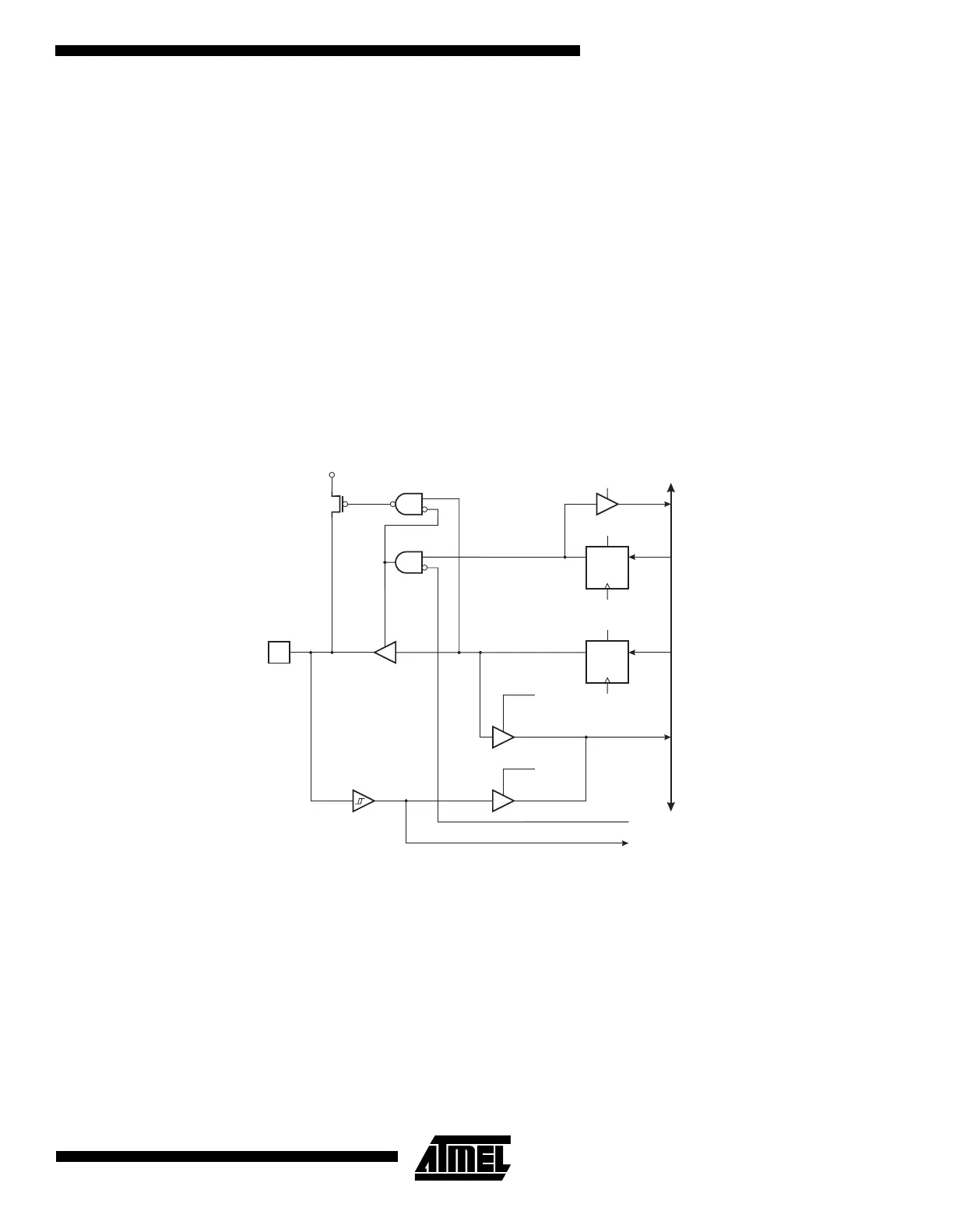
RXD - Port D, Bit 0
Receive Data (Data input pin for the UART). When the UART receiver is enabled this pin is configured as an input regard-
less of the value of DDRD0. When the UART forces this pin to be an input, a logical one in PORTD0 will turn on the internal
pull-up.
PortD Schematics
Note that all port pins are synchronized. The synchronization latches are however, not shown in the figures.
Figure 53. Port D Schematic Diagram (Pin PD0)
DATA BUS
D
D
Q
Q
RESET
RESET
C
C
WD
WP
RD
MOS
PULL-
UP
PD0
RXD
RXEN
WP:
WD:
RL:
RP:
RD:
RXD:
RXEN:
WRITE PORTD
WRITE DDRD
READ PORTD LATCH
READ PORTD PIN
READ DDRD
UART RECEIVE DATA
UART RECEIVE ENABLE
DDD0
PORTD0
RL
RP

 Loading...


