AT90S4414/8515
18
Note: Reserved and unused locations are not shown in the table
All AT90S4414/8515 I/Os and peripherals are placed in the I/O space. The I/O locations are accessed by the IN and OUT
instructions transferring data between the 32 general purpose working registers and the I/O space. I/O registers within the
address range $00 - $1F are directly bit-accessible using the SBI and CBI instructions. In these registers, the value of
single bits can be checked by using the SBIS and SBIC instructions. Refer to the instruction set chapter for more details.
When using the I/O specific commands IN, OUT the I/O addresses $00 - $3F must be used. When addressing I/O registers
as SRAM, $20 must be added to this address. All I/O register addresses throughout this document are shown with the
SRAM address in parentheses.
For compatibility with future devices, reserved bits should be written to zero if accessed. Reserved I/O memory addresses
should never be written.
Some of the status flags are cleared by writing a logical one to them. Note that the CBI and SBI instructions will operate on
all bits in the I/O register, writing a one back into any flag read as set, thus clearing the flag. The CBI and SBI instructions
work with registers $00 to $1F only.
The I/O and peripherals control registers are explained in the following chapters.
Status Register - SREG
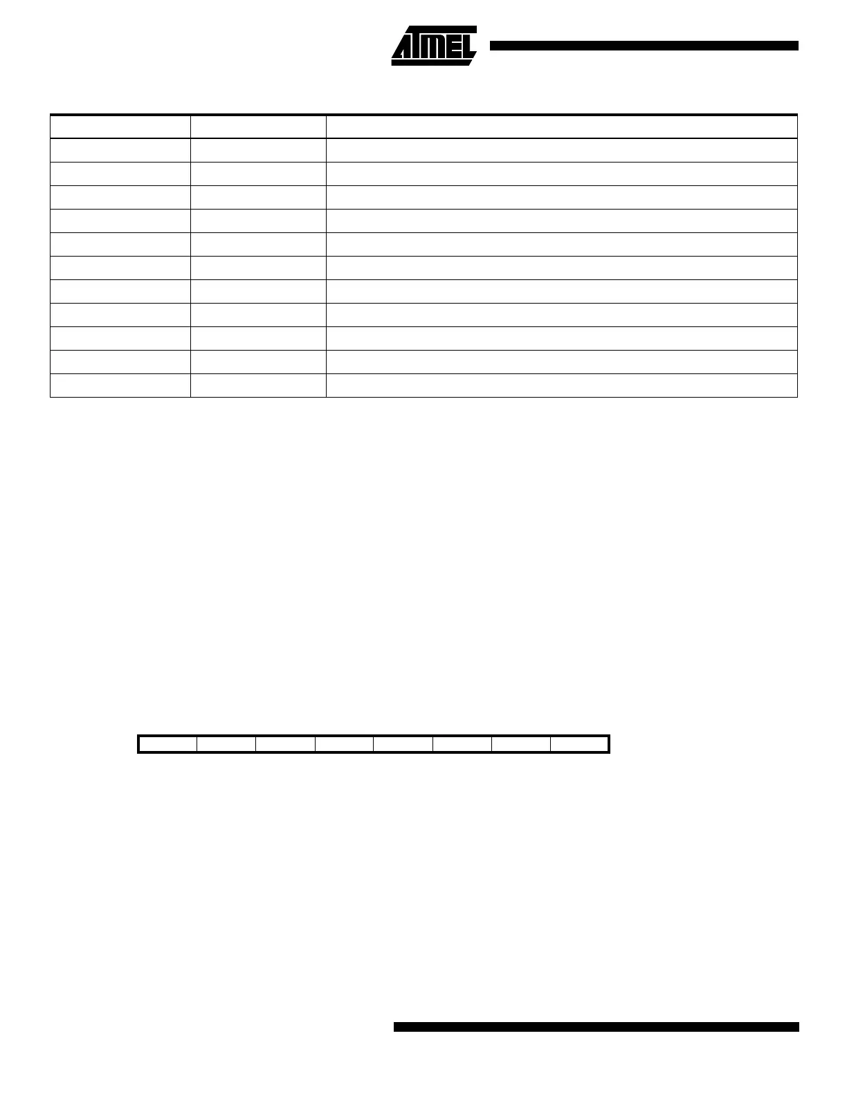
The AVR status register - SREG - at I/O space location $3F ($5F) is defined as:
•
Bit 7 - I: Global Interrupt Enable
The global interrupt enable bit must be set (one) for the interrupts to be enabled. The individual interrupt enable control is
then performed in separate control registers. If the global interrupt enable bit is cleared (zero), none of the interrupts are
enabled independent of the individual interrupt enable settings. The I-bit is cleared by hardware after an interrupt has
occurred, and is set by the RETI instruction to enable subsequent interrupts.
•
Bit 6 - T: Bit Copy Storage
The bit copy instructions BLD (Bit LoaD) and BST (Bit STore) use the T bit as source and destination for the operated bit.
A bit from a register in the register file can be copied into T by the BST instruction, and a bit in T can be copied into a bit in
a register in the register file by the BLD instruction.
$12 ($32) PORTD Data Register, Port D
$11 ($31) DDRD Data Direction Register, Port D
$10 ($30) PIND Input Pins, Port D
$0F ($2F) SPDR SPI I/O Data Register
$0E ($2E) SPSR SPI Status Register
$0D ($2D) SPCR SPI Control Register
$0C ($2C) UDR UART I/O Data Register
$0B ($2B) USR UART Status Register
$0A ($2A) UCR UART Control Register
$09 ($29) UBRR UART Baud Rate Register
$08 ($28) ACSR Analog Comparator Control and Status Register
Bit 76543210
$3F ($5F) I T H S V N Z C SREG
Read/Write R/W R/W R/W R/W R/W R/W R/W R/W
Initial value 0 0 0 0 0 0 0 0
Table 2. AT90S4414/8515 I/O Space (Continued)
Address Hex Name Function

 Loading...


