AT90S4414/8515
27
MCU Control Register - MCUCR
The MCU Control Register contains control bits for general MCU functions.
•
Bit 7 - SRE: External SRAM Enable
When the SRE bit is set (one), the external data SRAM is enabled, and the pin functions AD0-7 (Port A), A8-15 (Port C),
WR
and RD (Port D) are activated as the alternate pin functions. Then the SRE bit overrides any pin direction settings in
the respective data direction registers. See “The SRAM Data Memory - Internal and External” for description of the External
SRAM pin functions. When the SRE bit is cleared (zero), the external data SRAM is disabled, and the normal pin and data
direction settings are used.
•
Bit 6 - SRW: External SRAM Wait State
When the SRW bit is set (one), a one cycle wait state is inserted in the external data SRAM access cycle. When the SRW
bit is cleared (zero), the external data SRAM access is executed with the normal three-cycle scheme. See Figure 43: Exter-
nal Data SRAM Memory Cycles without Wait State and Figure 44: External Data SRAM Memory Cycles with Wait State.
•
Bit 5 - SE: Sleep Enable
The SE bit must be set (one) to make the MCU enter the sleep mode when the SLEEP instruction is executed. To avoid the
MCU entering the sleep mode unless it is the programmers purpose, it is recommended to set the Sleep Enable SE bit just
before the execution of the SLEEP instruction.
•
Bit 4 - SM: Sleep Mode
This bit selects between the two available sleep modes. When SM is cleared (zero), Idle Mode is selected as Sleep Mode.
When SM is set (one), Power Down mode is selected as sleep mode. For details, refer to the paragraph “Sleep Modes”
below.
•
Bit 3, 2 - ISC11, ISC10: Interrupt Sense Control 1 bit 1 and bit 0
The External Interrupt 1 is activated by the external pin INT1 if the SREG I-flag and the corresponding interrupt mask in the
GIMSK is set. The level and edges on the external INT1 pin that activate the interrupt are defined in the following table:
Note: When changing the ISC11/ISC10 bits, INT1 must be disabled by clearing its Interrupt Enable bit in the GIMSK Register.
Otherwise an interrupt can occur when the bits are changed.
• Bit 1, 0 - ISC01, ISC00: Interrupt Sense Control 0 bit 1 and bit 0
The External Interrupt 0 is activated by the external pin INT0 if the SREG I-flag and the corresponding interrupt mask is set.
The level and edges on the external INT0 pin that activate the interrupt are defined in the following table:
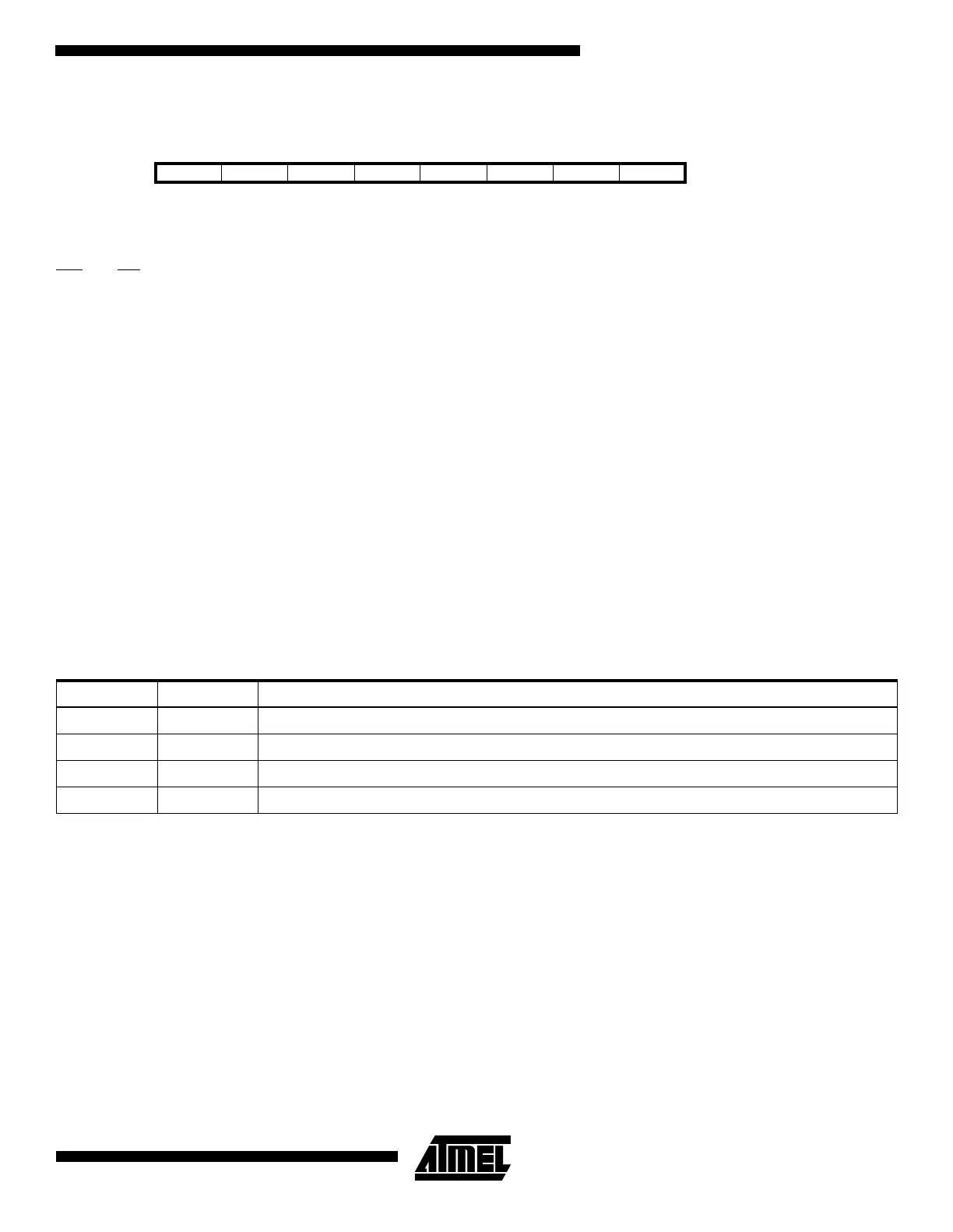
Bit 76543210
$35 ($55) SRE SRW SE SM ISC11 ISC10 ISC01 ISC00 MCUCR
Read/Write R/W R/W R/W R/W R/W R/W R/W R/W
Initial value 0 0 0 0 0 0 0 0
Table 6. Interrupt 1 Sense Control
ISC11 ISC10 Description
0 0 The low level of INT1 generates an interrupt request.
01Reserved
1 0 The falling edge of INT1 generates an interrupt request.
1 1 The rising edge of INT1 generates an interrupt request.

 Loading...


