ATtiny15L
52
Note: a = address high bits
b = address low bits
i = data in
o = data out
x = don’t care
1 = Lock Bit1
2 = Lock Bit2
3 = CKSEL0 Fuse
4 = CKSEL1 Fuse
5 = RSTDSBL Fuse
6 = SPIEN Fuse
7 = BODEN Fuse
8 = BODLEVEL Fuse
The Lock bits can only be cleared by executing a Chip Erase.
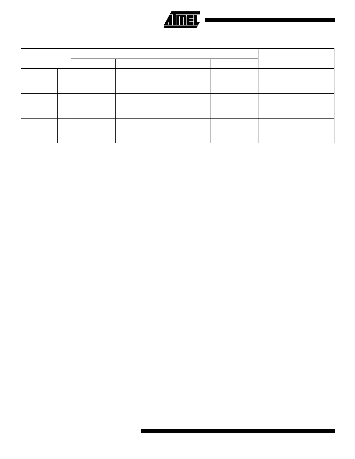
Read Lock bits
PB0
PB1
PB2
0_0000_0100_00
0_0100_1100_00
x_xxxx_xxxx_xx
0_0000_0000_00
0_0111_1000_00
x_xxxx_xxxx_xx
0_0000_0000_00
0_0111_1100_00
x_xxxx_21xx_xx
Reading 2, 1 = “0” means the Lock
bit is programmed
Read Signature
Bytes
PB0
PB1
PB2
0_0000_1000_00
0_0100_1100_00
x_xxxx_xxxx_xx
0_0000_00bb_00
0_0000_1100_00
x_xxxx_xxxx_xx
0_0000_0000_00
0_0110_1000_00
x_xxxx_xxxx_xx
0_0000_0000_00
0_0110_1100_00
o_oooo_ooox_xx
Repeat Instr.2 - Instr.4 for each
Signature byte address
Read
Calibration Byte
PB0
PB1
PB2
0_0000_1000_00
0_0100_1100_00
x_xxxx_xxxx_xx
0_0000_0000_00
0_0000_1100_00
x_xxxx_xxxx_xx
0_0000_0000_00
0_0111_1000_00
x_xxxx_xxxx_xx
0_0000_0000_00
0_0111_1100_00
o_oooo_ooox_xx
Table 24. High-voltage Serial Programming Instruction Set for ATtiny15L (Continued)
Instruction
Instruction Format
Operation RemarksInstr.1 Instr.2 Instr.3 Instr.4
 Loading...


