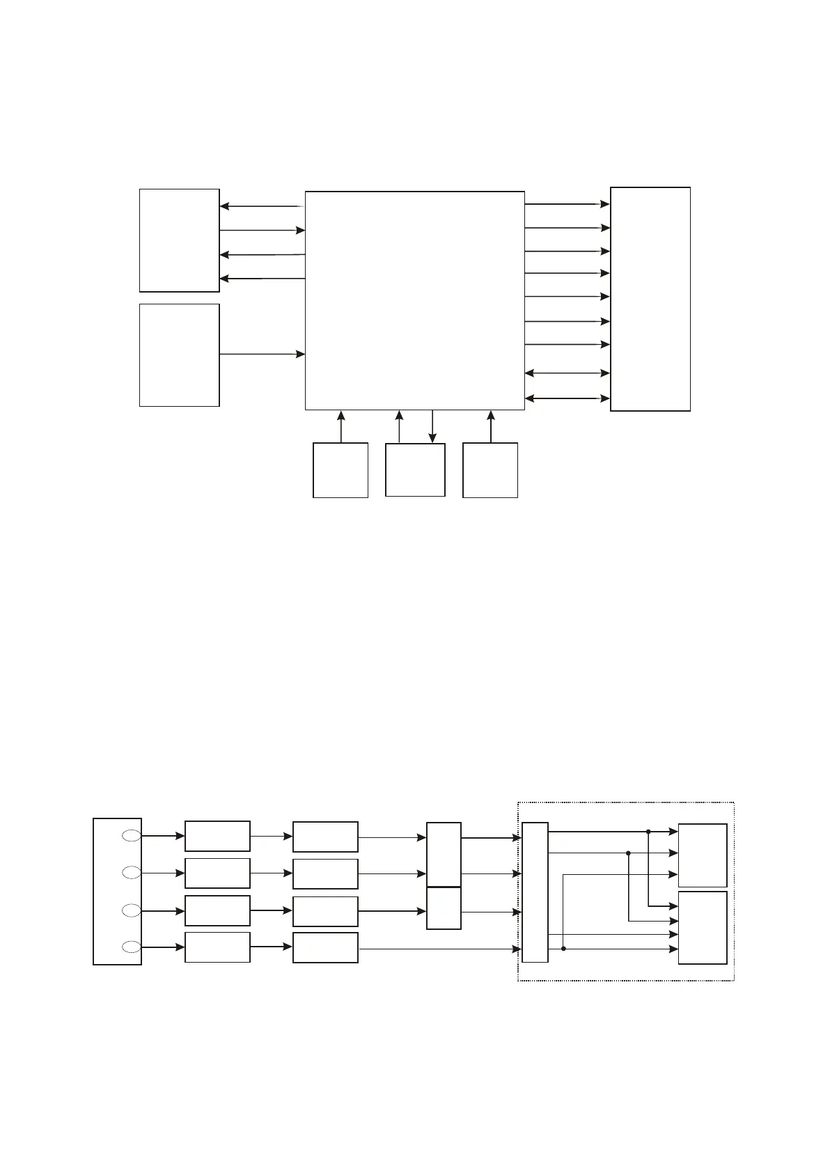
4.2 Decode Circuit
Decode circuit is mainly composed of MT1389,SDRAM and FLASH. Block diagram of circuit is
shown in figure 4.2.1.
SDRAM
SDCLK
SDCKE
DCS
DRAS
SWE
DQM0
DQM1
DQ0~DQ15
MA0~MA11
URST
SF_CS
SF_DO
SF_DI
MT 1389L
FLASH
Reset Circuit
1.8V
voltage
stabilizing
V18
27M Clock
Figure 4.2.1 Block diagram of decode circuit
3.3V
voltage
stabilizing
DV33
SF_CK
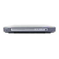
4.3 Video Circuit
.3.1.
MT1389L has video D/A converter circuit and video output has R/B/G, Y/Pb/Pr, Y/Cb/Cr, CVBS and
Y/C output modes, in which R/B/G, Y/Pb/Pr, Y/Cb/Cr and Y/C can not output at the same time and need
to be switched via software. CVBS is a separate output mode; four channel video signal is outputted to
AV board by MT1389 after video filtering and clamping. Block diagram of video signal process is shown
in figure 4
Figure 4.3.1 Block diagram of video signal process
MT1389L
103
102
99
V_B
L19
V_G
D6
CVBS
D18
VIDEO_SY
VIDEO_SC
VIDEO_G/Y
PB#
PR#
VIDEO#
S
te
r
m
i
n
al
J
K1
SCART
104
L17
L18
D11
D10
Video
component
V_R
L16
V
id
e
o
t
e
r
min
al
VIDEO_CVBS
Y1
VIDEO_B/U
VIDEO_R/V
Y1#
XS701
RGB_CVBS
- 18 -