5
5
4
4
3
3
2
2
1
1
D D
C C
B B
A A
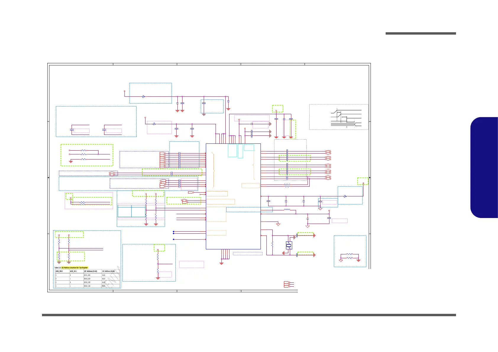
DCI debug interface
Internal 45K ohm pull-down.
Note:
Both SSTx and SSRx between USB host
and ANX7440 need AC capacitors.
USB host SSTx connects to ANX7440 SSRx.
USB host SSRx connects to ANX7440 SSTx.
The capacitors should be placed
near SSTx pin.
Note:
AC capacitors for DP
main link should be put
close to DP source
Chock chooses 3.3uH;
>500mA
DCR<100mOhm.
Internal DC-DC 0.9v
output: Maximum 500mA
Signal GND and
GND_DCDC must be
separated. They
are connected at
a single point.
Close to
USB TYPE-C Conn.
OP_MODE_1/O MODE
00 Disabled
01 USB3(default)
10 DP
11 USB3 + DP
USB3.1/DP MUX ANX7440
20180709 Modify
DIFF=90ohm, L<6"
From
NV Port_F
USB3.1 Gen2 from PCH
DIFF= 80ohm, L<5"
Note:
Capacitors
close to pin21
Ferrite Beads choose low DCR parts.
might choose, but not limited to:
BKP1608HS600-T
BLM18SG221TN1
BLM18SG121TN1
Output
FLIP:
USB Typc-C Orientation:
0=normal, 1=flipped
CC1 detection is normal
or
CC2 detection is flipped
Compatible with 3.3V input.
Layout rules:
1. Place ANX7440/30/90/96 and USB Type-C/Type-A connector in an open area for
easier routing.
2. High-speed trace should be routed with high-priority.
3. If using internal DC/DC, create a dedicated DC/DC VGND
4. High-speed trace must keep distance from DC/DC and other noise source. RX
to TX spacing should be >20mils.
5. High-speed trace must be continuous and without stub, especially to RX
traces.
6. Ground void should be applied to wide pad along the high-speed traces.
7. ESD ground should be wide.
8. Every AVDD09 pin must have a 0.01uF decoupling capacitor that is very
close.
9. AVDD09 power delivery must be wide and away from noisy signal.
Note:
1. These capacitors are used to reduce the slew rate of AUX CH to
meet the DP V1.4 AUX CH requirement.
2. These capacitors are mandatory for HBR3 application, for HBR2
and lower, the caps are optional.
3. Both the upstream and downstream port need to add the
capacitor for HBR3 application.
VDD_IO/VDD33
VDD18
t0 0ms
ʁ
POWER_EN
t1 0ms
ʁ
FLIP/OP_MODE
t2>12ms
ANX7440 PWR ON SEQ
VALID
ESR<20mOhm.
600ohm,
1.3A,
DCR=0.15ohm
220ohm,
2.5A,
DCR=0.04ohm
20180719 Modify from 3.3V to 1.8VA
PWR Rail=
VDD33
PWR Rail=
AVDD09
PWR Rail=
AVDD09
PWR Rail=
VDD_IO
PWR Rail=
VDD_IO
Compatible w/3.3V input
PWR Rail=
VDD33
20180719
Del ANX7440_PWER_EN RC
max=
509mA
max=
1.1mA
max=
0.0096mA
20180719
Modify C value
20180720
FAE recommend
20180720
FAE recommend
20180723 FAE recommend
20180723 FAE recommend
20180723 FAE recommend
20180727
MLCC Comm part
20180727
MLCC Comm part
down sizedown size
down size
down size
From Nv
DIFF=90ohm, L<6"
D01A 0903 Change footprint
D02 0914
D02 0914
D02 0914
D02 0914
D02 0914
D02 0914
D02 0928 follow P95
D02 0928 follow P95
D02 0928 follow P95
D02 0928 follow P95
D02 0928 follow P95
D02 0928 follow P95
D02 1004
D02 1008 FAE recommend
D02 1017
D02 1017
3.3V
ANX_1.8V
VDD0.9_LEX
ANX_1.8V ANX_1.8V
ANX_1.8V
GND_DCDC
GND_DCDC
GND_DCDC
GND_DCDC
VDD0.9_LEX
ANX_1.8V
ANX_1.8V ANX_1.8V
3.3V
ANX_1.8V
VDD0.9_LEX
3.3V
NV3V3
TYPEC_TX2- 51
TYPEC_TX1+ 51
TYPEC_TX1- 51
TYPEC_TX2+ 51
TYPEC_SBU2 51
TYPEC_SBU1 51
3.3V3,10,15,49,51,60,62,63,64,65,68,70,71,72
ANX_1.8V10
ANX7440_POWER_EN51
MDP_F#027
MDP_F027
MDP_F#127
MDP_F127
MDP_F#227
MDP_F227
MDP_F#327
MDP_F327
TYPEC_RX1+ 51
TYPEC_RX1- 51
TYPEC_RX2+ 51
TYPEC_RX2- 51
USB3_RX139
USB3_RX1#39
USB3_TX139
USB3_TX1#39
ANX7440_SDA51
ANX7440_SCL51
MDP_F_AUX_SCL27
MDP_F_AUX#_SDA27
NV3V311,12,15,28,29,31,64,74,75
Title
Size Document Number Rev
Date: Sheet
of
6-71-PB500-D03
D03
[50] USB3.1/DP MUX ANX7440
A3
50 91Friday, December 07, 2018
ᙔ!Ϻ!ႝ!တ!!DMFWP!DP/
PB50EF
Title
Size Document Number Rev
Date: Sheet
of
6-71-PB500-D03
D03
[50] USB3.1/DP MUX ANX7440
A3
50 91Friday, December 07, 2018
ᙔ!Ϻ!ႝ!တ!!DMFWP!DP/
PB50EF
Title
Size Document Number Rev
Date: Sheet
of
6-71-PB500-D03
D03
[50] USB3.1/DP MUX ANX7440
A3
50 91Friday, December 07, 2018
ᙔ!Ϻ!ႝ!တ!!DMFWP!DP/
PB50EF
R872 100K_1%_04
L8 HCB1005KF-121T20
P/N = 6-19-31001-275
DCR = 0.1ohm
Impedance = 120ohm
Rated Current = 2A
R28 1.8K_1%_04
X3
FSX3M_24MHZ
21
34
C1172 0.22u_10V_X5R_04
C1226 0.22u_10V_X5R_04
R39
*4.7K_04
C55
1000p_50V_X7R_04
C1245 0.1u_10V_X7R_04
R493
*4.7K_04
C45
4.7u_6.3V_X5R_04
C1249 0.1u_10V_X7R_04
C40
0.01u_16V_X7R_04
C1584 0.33u_6.3V_X5R_04
L29 HCB1608KF-300T60
P/N = 6-19-31001-275
DCR = 0.04ohm
Impedance = 125ohm
Rated Current = 3A
R56 0_06
C68
22u_6.3V_X5R_06
C1248 0.1u_10V_X7R_04
Analogix Semi
ANX7440QN-CB-R
U35
PCB Footprint = qfn60-7x7mmb-1
AVDD09_1
1
ML2P
2
ML2N
3
AVSS_4
4
ML3P
5
ML3N
6
POWER_EN
7
AUXP
8
AUXN
9
DVDD09_10
10
VDD_IO_11
11
VGND
12
VX
13
VIN
14
VFB
15
RX1N
16
RX1P
17
AVSS_18
18
TX1P
19
TX1N
20
AVDD09_21
21
VDD18_22
22
TX2N
23
TX2P
24
AVSS_25
25
RX2N
26
RX2P
27
TEST_R
28
FLIP
29
XTAL_I
30
XTAL_O
31
VDD18_32
32
SBU2
33
SBU1
34
I2C_ADR_SEL1
35
I2C_ADR_SEL0
36
SCL
37
SDA
38
VDD_IO_39
39
TEST_EN
40
DVDD09_41
41
OP_MODE_1
42
OP_MODE_0
43
PULL_1
45
PULL_2
44
DCI_DAT
46
DCI_CLK
47
VDD18_48
48
SSRXN
49
SSRXP
50
AVDD09_51
51
SSTXN
52
SSTXP
53
VDD33
54
ML0P
55
ML0N
56
AVSS_57
57
ML1P
58
ML1N
59
VDD18_60
60
DVSS
61
C1585 0.33u_6.3V_X5R_04
C1171
18p_25V_NPO_02
C1222 0.22u_10V_X5R_04
C1206
1000p_50V_X7R_04
R63 0_06
R40
4.7K_04
C1240
4.7u_6.3V_X5R_04
C1224 0.22u_10V_X5R_04
C91
18p_25V_NPO_02
C37
1u_6.3V_X5R_02
C1199
0.1u_6.3V_X5R_02
C17 0.22u_10V_X5R_04
C1229 0.1u_10V_X7R_04
C46 1u_6.3V_X5R_02
C19 0.1u_10V_X7R_04
R48
*4.7K_04
C1209 10p_50V_NPO_04
C1227 0.1u_10V_X7R_04
C97
22u_6.3V_X5R_06
R26
*4.7K_04
C1225 0.22u_10V_X5R_04
L7 HCB1608KF-300T60
P/N = 6-19-31001-275
DCR = 0.04ohm
Impedance = 125ohm
Rated Current = 3A
R47
4.7K_04
C1216 10p_50V_NPO_04
C1250 0.1u_10V_X7R_04
C67
0.1u_25V_X7R_06
C16 0.22u_10V_X5R_04
C35
1u_6.3V_X5R_02
C99
0.1u_25V_X7R_06
C1230 0.1u_10V_X7R_04
C1586 0.33u_6.3V_X5R_04
R511 *100K_1%_04
R27
*4.7K_04
L30
AHP252012RA-3R3M
ahp252012ra-xxxm
P/N = 6-19-41001-049
C44 1000p_50V_X7R_04
C1587 0.33u_6.3V_X5R_04
C1232 0.1u_10V_X7R_04
C98
10u_6.3V_X5R_06
R488
1M_04
C48
1000p_50V_X7R_04
C42 0.1u_6.3V_X5R_02
R38
4.7K_04
C1247 0.1u_10V_X7R_04
R512 100K_1%_04
R473 100K_04
C18 0.1u_10V_X7R_04
C54
1000p_50V_X7R_04
R31 1.8K_1%_04
R474 100K_04
R37
4.7K_04
C1173 0.22u_10V_X5R_04
C1246 0.1u_10V_X7R_04
R491
4.7K_04
AAUX_SCL
AAUX#_SDA
ANX7440_SDA
ANX7440_SCL
ANX7440_I2C_ADR_SEL0
ANX7440_I2C_ADR_SEL1
ANX7440_I2C_ADR_SEL1
ANX7440_I2C_ADR_SEL0
ANX7440_FLIP
ANX7440_OP_MODE_1
ANX7440_OP_MODE_0
TYPEC_SBU1
TYPEC_SBU2
ANX7440_FLIP
TYPEC_SBU1
TYPEC_SBU2MDP_F_AUX#_SDA
MDP_F_AUX_SCL
AAUX_SCL
ANX7440_SDA
ANX7440_SCL
MDP_F_AUX_SCL
MDP_F_AUX#_SDA
AAUX#_SDA