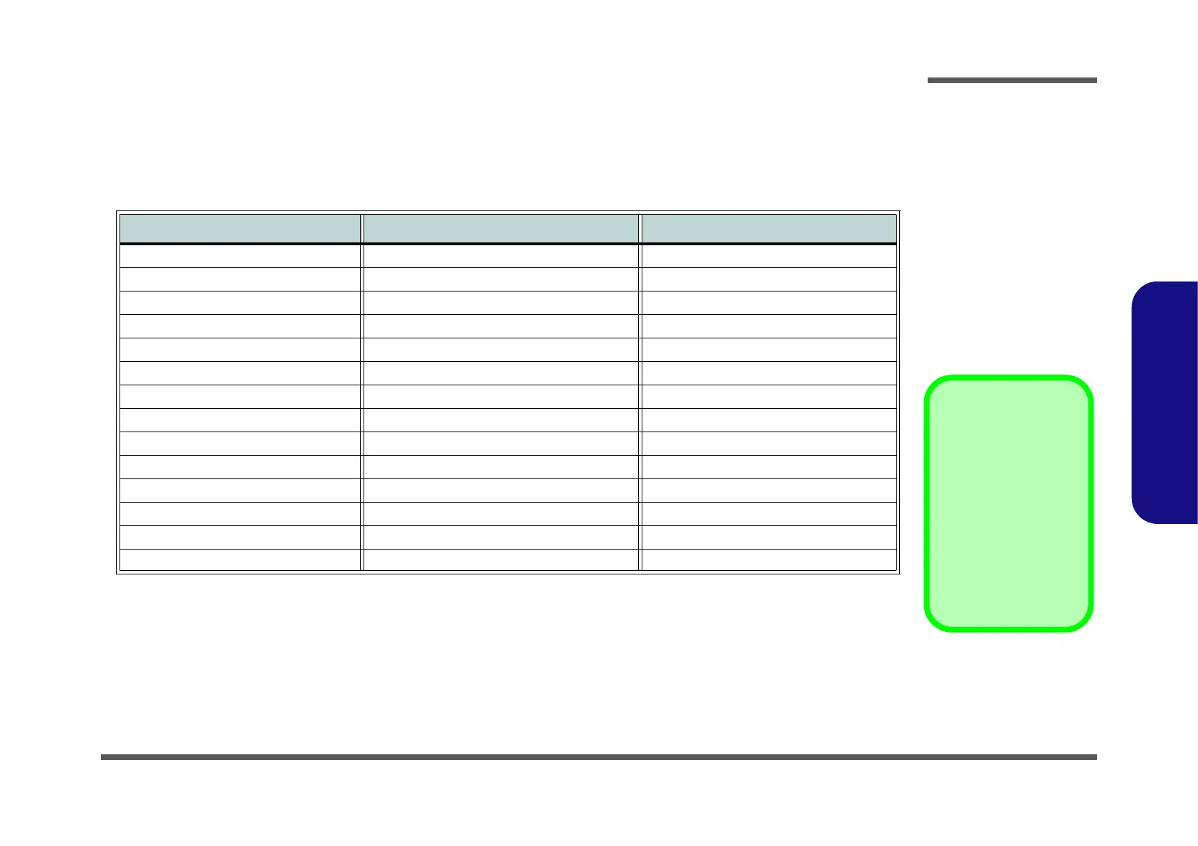
Schematic Diagrams
B - 1
B.Schematic Diagrams
Appendix B: Schematic Diagrams
Table B - 1
SCHEMATIC
DIAGRAMS
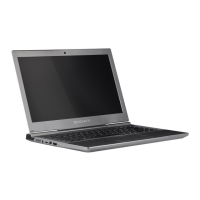
This appendix has circuit diagrams of the W740SU notebook’s PCB’s. The following table indicates where to find the
appropriate schematic diagram.
Diagram - Page Diagram - Page Diagram - Page
System Block Diagram - Page B - 2 PCH 1/10 - RTC, HDA, SATA - Page B - 16 KBC-ITE IT8587E - Page B - 30
TPM - Page B - 3 PCH 2/10 - LPC, SMBUS SPI, CL - Page B - 17 5VS, 3.3VS, 5V, 3.3V, VCCDDQ - Page B - 31
Processor 1/7-DMI, FDI, PEG - Page B - 4 PCH 3/10 - DMI, FDI, PWRGD - Page B - 18 1.05V - Page B - 32
Processor 2/7- CLK, MISC - Page B - 5 PCH 4/10 - CRT, Display, PCI - Page B - 19 VDD3, VDD5, 3.3VM - Page B - 33
Processor 3/7- (DDR3) - Page B - 6 PCH 5/10 - PCIe, USB - Page B - 20 VDDQ, VDDQ_VTT, 1.5VS - Page B - 34
Processor 4/7- Display - Page B - 7 PCH 6/10 - GPIO, Misc - Page B - 21 VCORE - Page B - 35
Processor 5/7- Power - Page B - 8 PCH 7/10 - CLK - Page B - 22 AC-IN, Charger - Page B - 36
Processor 6/7- GND - Page B - 9 PCH 8/10 - POWER - Page B - 23 POWER SWITCH BOARD - Page B - 37
Processor 7/7- RSVD - Page B - 10 PCH 9/10 - Power - Page B - 24 HDD Board - Page B - 38
DDR3 SO-DIMM_0 - Page B - 11 PCH 10/10 - GND - Page B - 25 LED Board - Page B - 39
DDR3 SO-DIMM_1 - Page B - 12 WLAN, mSATA - Page B - 26 Card Reader - Page B - 40
PANEL - Page B - 13 CCD, FAN, CLICK - Page B - 27 USB - Page B - 41
HDMI - Page B - 14 LAN, RJ-45 - Page B - 28 USB, Audio Board - Page B - 42
Mini Display Port - Page B - 15 VT1802S - Page B - 29 Power Diagram - Page B - 43
Version Note
The schematic dia-
grams in this chapter
are based upon ver-
sion 6-7P-W7405-004.
If your mainboard (or
other boards) are a lat-
er version, please
check with the Service
Center for updated di-
agrams (if required).