1541 CIRCUIT THEORY
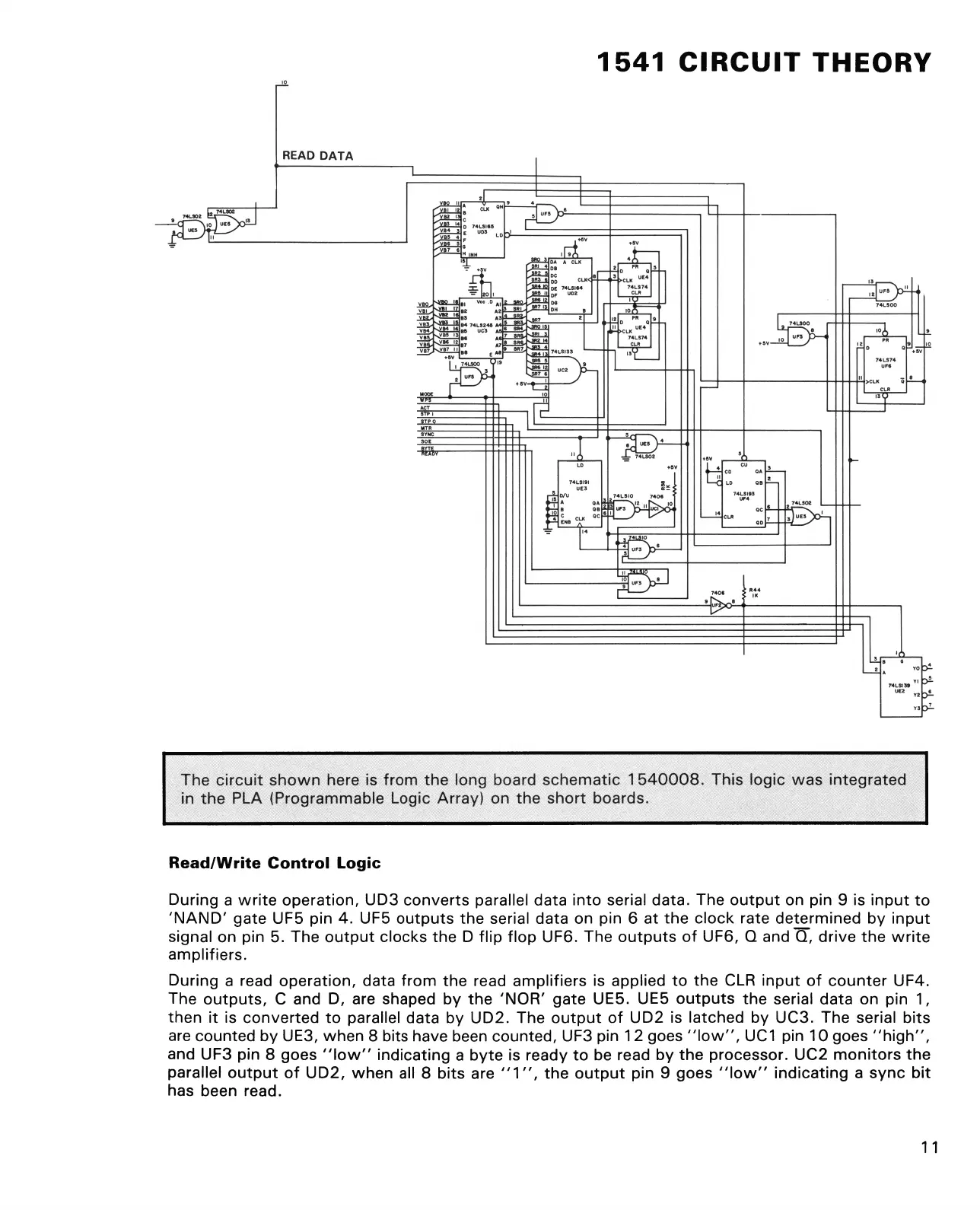
Read/Write Control Logic
During a write operation, UD3 converts parallel data into serial data. The output on pin 9 is input to
'NAND' gate UF5 pin 4. UF5 outputs the serial data on pin 6 at the clock rate determined by input
signal on pin 5. The output clocks the D flip flop UF6. The outputs of UF6, Q and Q, drive the write
amplifiers.
During a read operation, data from the read amplifiers is applied to the CLR input of counter UF4.
The outputs, C and D, are shaped by the 'NOR' gate UE5. UE5 outputs the serial data on pin 1,
then it is converted to parallel data by UD2. The output of UD2 is latched by UC3. The serial bits
are counted by UE3, when 8 bits have been counted, UF3 pin 12 goes ''low'', UC1 pin 10 goes ''high'',
and UF3 pin 8 goes "low” indicating a byte is ready to be read by the processor. UC2 monitors the
parallel output of UD2, when all 8 bits are ” 1” , the output pin 9 goes "low” indicating a sync bit
has been read.