MA-2402 Service Manual
4-2 Circuit Theory
130445-1 Rev. A
©2000 Crown International, Inc.
dition which in turn results in high peak output voltage.
The output of the Error Amp, called the Error Signal (ES)
drives the Voltage Translators.
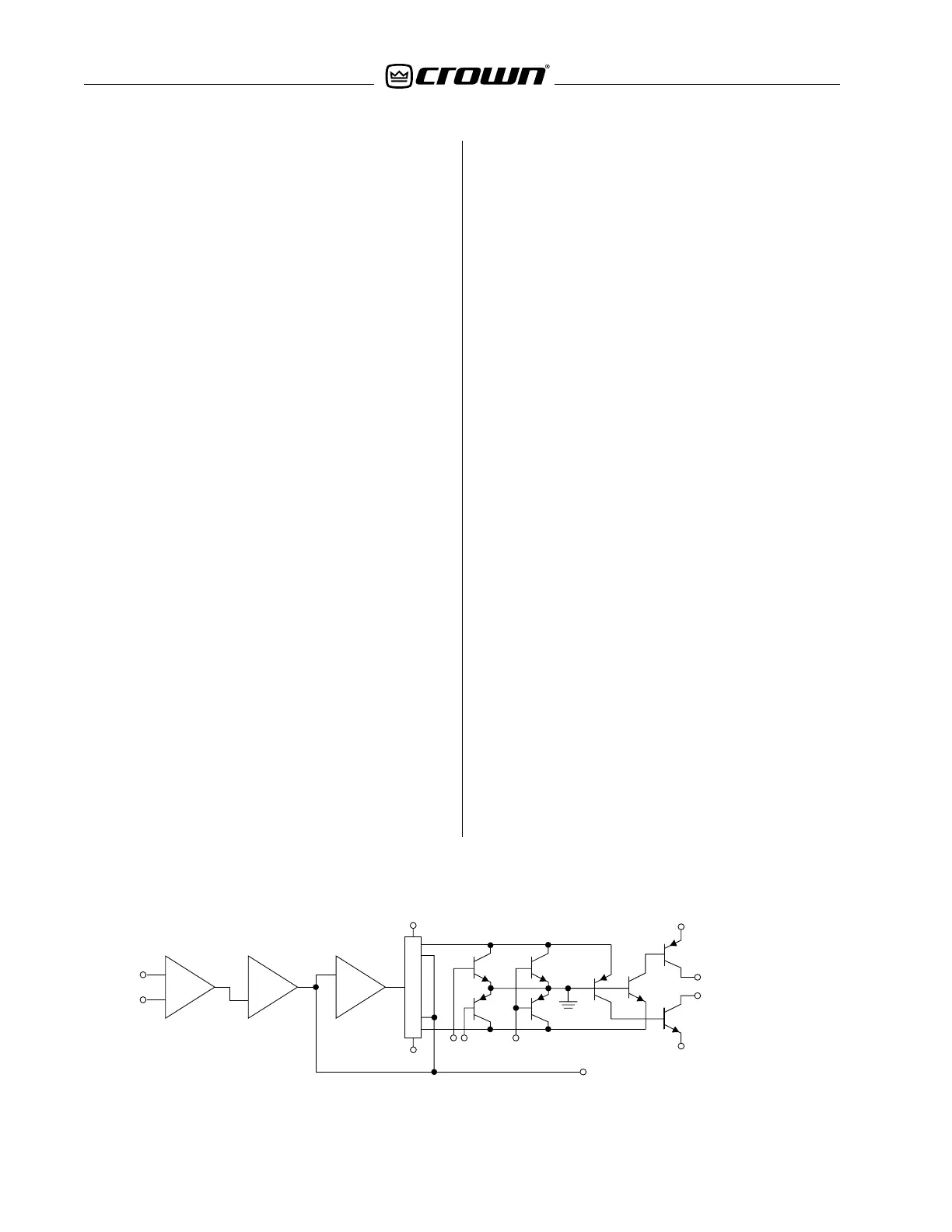
4.4 Voltage Amplification
The Voltage Translator stage separates the output of
the Error Amp into balanced positive and negative drive
voltages for the Last Voltage Amplifiers (LVAs), translat-
ing the signal from ground referenced ±15V to ±Vcc
reference. LVAs provide the main voltage amplification
and drive the High Side output stages. Gain from Volt-
age Translator input to amplifier output is a factor of
25.2.
4.4.1 Voltage Translators
A voltage divider network splits the Error Signal (ES)
into positive and negative drive signals for the balanced
voltage translator stage. These offset reference voltages
drive the input to the Voltage Translator transistors. A
nested NFb loop from the output of the amplifier mixes
with the inverted signal riding on the offset references.
This negative feedback fixes gain at the offset refer-
ence points (and the output of the Error Amp) at a fac-
tor of –25.2 with respect to the amplifier output. The
Voltage Translators are arranged in a common base
configuration for non-inverting voltage gain with equal
gain. They shift the audio from the ±15V reference to
VCC reference. Their outputs drive their respective LVA.
Also tied into the Voltage Translator inputs are ODEP
limiting transistors and control/protection transistors. The
ODEP transistors steal drive as dictated by the ODEP
circuitry (discussed later). The control/protection tran-
sistors act as switches to totally shunt audio to ground
during the turn-on delay, or during a DC/LF or Fault pro-
tective action.
4.4.2 Last Voltage Amplifiers (LVAs)
The Voltage Translator stage channels the signal to the
Last Voltage Amplifiers (LVA’s) in a balanced configura-
tion. The +LVA and -LVA, with their push-pull effect
through the Bias Servo, drive the fully complementary
output stage. The LVAs are configured as common
emitter amplifiers. This configuration provides sufficient
voltage gain and inverts the audio. The polarity inver-
sion is necessary to avoid an overall polarity inversion
from input jack to output jack, and it allows the NFb
loop to control Error Amp gain by feeding back to its
non-inverting input (with its polarity opposite to the out-
put of the VGS). With the added voltage swing provided
by the LVAs, the signal then gains current amplification
through the Darlington emitter-follower output stage.
4.5 Grounded Bridge Topology
Figure 4.2 is a simplified example of the grounded bridge
output topology. It consists of four quadrants of three
deep Darlington (composite) emitter-follower stages per
channel: one NPN and one PNP on the High Side of the
bridge (driving the load), and one NPN and one PNP
on the Low Side of the bridge (controlling the ground
reference for the rails). The output stages are biased to
operate class AB+B for ultra low distortion in the signal
zero-crossing region and high efficiency.
4.5.1 High Side (HS)
The High Side (HS) of the bridge operates much like a
conventional bipolar push-pull output configuration. As
the input drive voltage becomes more positive, the HS
NPN conducts and delivers positive voltage to the load.
Eventually the NPN devices reach full conduction and
+Vcc is across the load. At this time the HS PNP is bi-
ased off. When the drive signal is negative going, the
HS PNP conducts to deliver –Vcc to the load and the
HS NPN stage is off.
+
-
+
-
+
-
BGS VGS Error
Amp
Audio
Inputs
Voltage Divider
NFb Loop
+
-
ODEP
Mute
+15V
-15V
+VCC
-VCC
NPN Outputs (+HS)
PNP Outputs (-HS)
Q100
Q103
Q121
Q122
Q101
Q102
Q105
Q110
Voltage
Translators
LVA's
Figure 4.1 Typical Amplifier Front End and Voltage Amplification Stages.