8: Synthesizer Board
8-4 PRC1099A-MS
8.2 Connector Pin Assignments
8.2.1 J1 Connector
J1 connects to the Processor board J3 connector through the Audio/Filter
board.
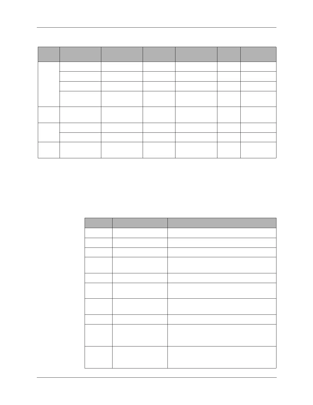
Table 8-1 Sample FTW Programming Values
Output Target F
o
Value Dec FTW Hex
Value
Actual F
o
Error in
Hz
% Error
1st LO 76,650,000.00 658,418,486.48 273EAB36 76,649,999.94 0.0555 7.24159E-08
86,650,000.00 744,317,832.40 2C5D6388 86,649,999.95 0.0462 5.33106E-08
96,650,000.00 830,217,178.32 317C1BDA 96,649,999.96 0.0369 6.81587E-08
105,650,000.0
0
901,943,132.16 35C28F5C 104,999,999.98 0.0186 1.77395E-08
2nd
LO
73,350,000.00 630,071,702.32 258E2196 73,349,999.96 0.0376 5.12957E-08
BFO 1,647,000.00 14,147,622.27 D7E026 1,646,999.97 0.0318 1.92957E-06
1,650,000.00 14,173,392.08 D844D0 1,649,999.99 0.0089 5.4186E-07
1.00 8.59 8 0.93 0.0687 6.86774253
8
Table 8-2 J1 Connector Pin Assignments
Pin Signal Description
1 GND Chassis ground.
2 GND Chassis ground.
3 ENM6C No connection.
4 SPI_DATA SPI data to U9, U11 and U18 from the
Processor board.
5 SPI_CLK SPI clock input from the Processor board
6 BITE Analog signal from phase detector to
Processor board.
7 +12V +12 VDC supply voltage from the Junction
board.
8 +5V No connection.
9 ENM6B Enable for address decoder U12 from the
Processor board through the Audio/Filter
board.
10 ENM6A Enables latch clock for shift register from the
Processor board through the Audio/Filter
board.