Service Manual
9
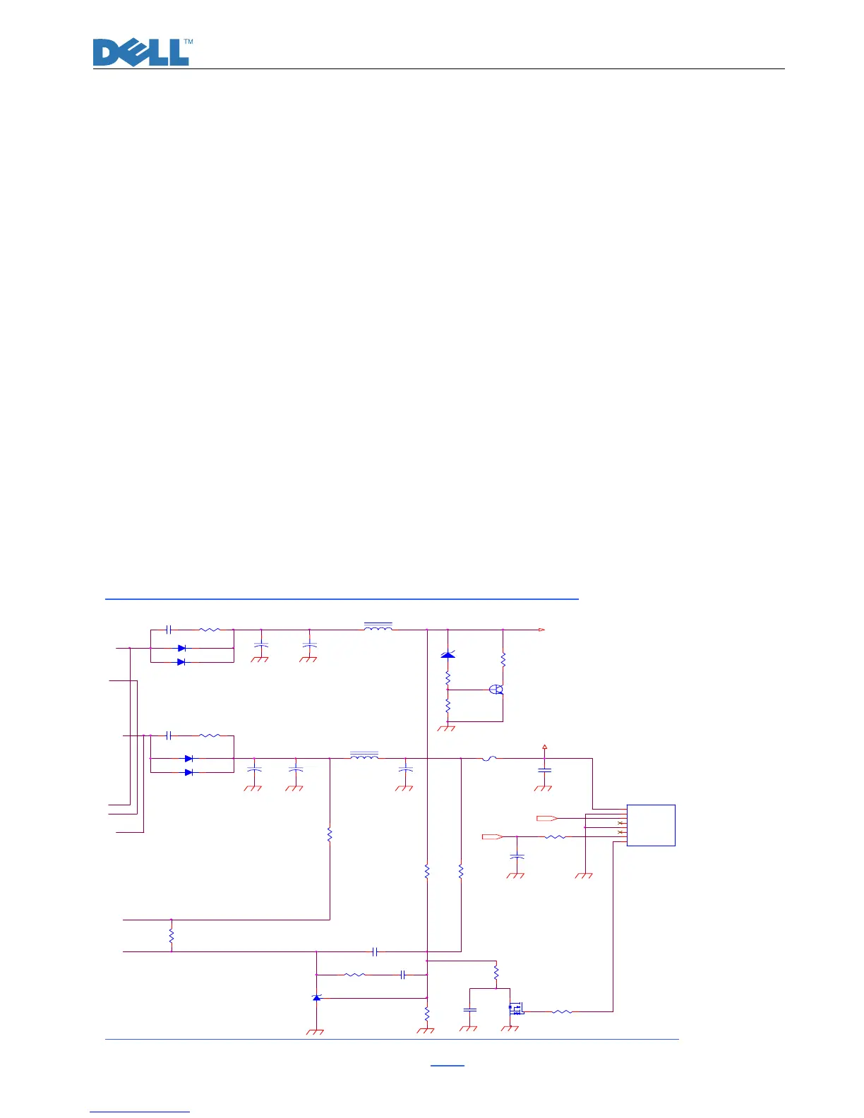
D850 is a rectifier in which there are 4 build-in diodes, inverting AC to DC.
C854 is used to smooth the wave from rectifier. R852 is a fuse resistor to protect the following circuit
when inrush current is too large.
U850 is a current-mode PWM controller with excellent power-saving opration,It features a
high-voltage current source to directly supply the startup current from bulk capacitor and further to provide
lossless startup circuit. Max start-up current for U850 is 100 uA, When current flow from the bulk
capacitor C854 through R843 and R842 gets to HV pin to start up U850, Meanwhile,the VCC supply
current is as low as 100 uA thus most of the HV current is utilized to change the VCC capacitor C855,
Whenever the Vcc voltage is higher than UVLO (16V),the GATE pin will output signal to drive the power
MOSFET(Q850), the high-voltage current source is off and the supply current is provided from the
auxiliary winding of the trasformer PIN5.
When U850 begins to operate Pin8 of U850 will output square wave to drive Q850, then the main
current flow get to GND bypassing through T850, Q850. Because of the change of current flow, wires in
the other side of T850 will induct current. In the same time, the current inducted by wires which connected
T850 Pin 1 and Pin 3, with components of D852, R856 and C855 ,will be supplied to U850 for normal
operating.
The typical current mode PWM controller feedbacks both current signal and voltage signal to close the
control loop and achieve ragulation.U850 detects the Q850 current from Isense pin which max voltage is
set as 0.85V, then the Q850 current can be calculated as:I peak=0.85V/R869,When the sense voltage
across the sense resistor R869, reaches the threshold voltage over 0.85V, the output GATE drive will be
turned off. R849 and C846 is used to avoid the Isen pin damaged by the negative turn-on spike.
The voltage feedback signal is provided from the TL431(I851) through the I850 to the COMP pin.When
the voltage on COMP pin is lower than 1.2V,the IC will turn off.
When Q850 is turned off, the main current flow will be consumed through D851, C875, R880, this will
prevent Q850 from being damaged under large current impulse and voltage spike.
RT pin is to program the switching frequency ,by connecting R846 to ground to set the switching frequency,f
=(65.0/R846)*100(KHz).
2.2.4) DC 12V and DC 5V Output Circuit and Feedback circuit:(fig.7)
+5V
DIM/ON/ OFF
C871
0.1/50V
Q890
2N7000/NC
G
DS
R871
270k
C890
0.1uF/50V/NC
R891
10K/NC
R867
270
+
C863
470u/25V
F85 1
5A/125V
R899 OPEN
+
C899
O PEN
+
C869
470u/25V
L851
CHK- 05 3
CN851
SIP-8P
6
1
2
5
3
4
7
8
+5V
+5V
GND
GND
DIM
ENA
PID
P- saving _on/off
Q851
2N4401/NC
E
B
C
C866
1000p/1KV
+12V
C876
0.1/50V
R866
10R 2W
L852
CHK- 05 3
I851
TL431
3
1
2
R862
10R 2W
R860
3K3 1%
R861
3K65 1%
D856 SR5-10
+
C868
470u/25V
R859
10K 1%
R858
5K1 1%
D855
NC/SF5-20
R886
10K/NC
C862
1000p/1KV
D854
SF5-20
D857 SR5-10
+
C867
470u/25V
C859
0.01/50V
R890
9.1K/NC
R887
10K/NC
+
C864
470u/25V
PID
R888
510R 2W/NC
ZD880
GDZ14B/NC
Fig.7