Service Manual
5
Chapter 3- CIRCUIT THEORY
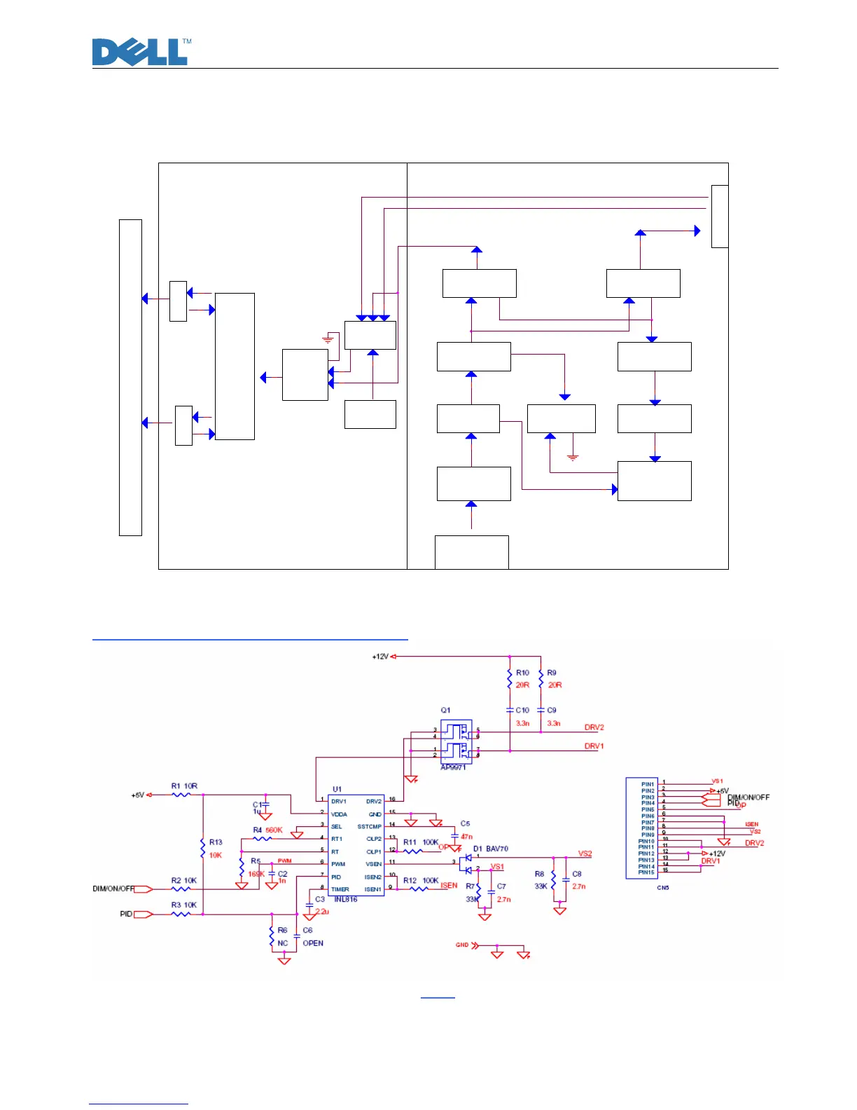
1. Block Diagram
This Block is comprised of interface board and switching power supplier board which is included by
inverter for CCFL
2. Electronic Circuit Theory
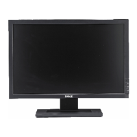
2.1 Inverter PWM circuit
2.1.1 Inverter Control circuit operations:(fig.2)
Fig.2
DC_5V through R1 and C1 will provide power for U1 on the pin2(VDDA),When the voltage at VDDA
is less than ~3.4V,the IC will enter the lockout mode. The IC will resume operation when the voltage at pin
VDDA exceeds an approximate 3.8V threshold.
Pin3(SEL) used to select appropriate drive topologies,connecting pin SEL to GED shows the IC in the
Snubber
&Schottky
+5V DC output
Brightness Control
Photocoupler
To Panel CCFL
Feedback
Control
AC Input
90V~264V
Power PWM
Control IC
Power
ON/OFF Control
Rectifier&
Filter
Circuit
Lamp2
Lamp1
To IF Board
Inverter
PWM IC
Snubber
&Schottky
Feedback
Transformer
MOSFET
Power
MOSFET
+12V DC output
Inverter
Transformer
AC Line Filter