


S
scottvanessaAug 19, 2025
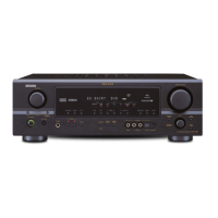
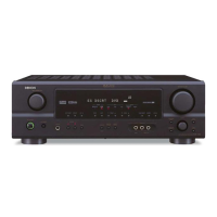
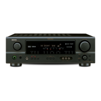
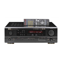
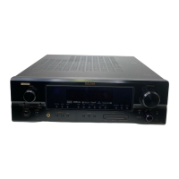
What to do if my Denon AVR-1907 display is on but there's no sound?
- QqmartinAug 19, 2025
If your Denon Stereo Receiver's display is lit but you're not getting any sound, there could be several reasons: * Check if the speaker cables are securely connected. * Ensure the FUNCTION knob is in the correct position. * Verify the volume isn't set to the minimum; turn it up. * Make sure MUTING is switched off. * Confirm a digital signal is being input and that you've selected the correct digital signal input source.