17
DN-D4500
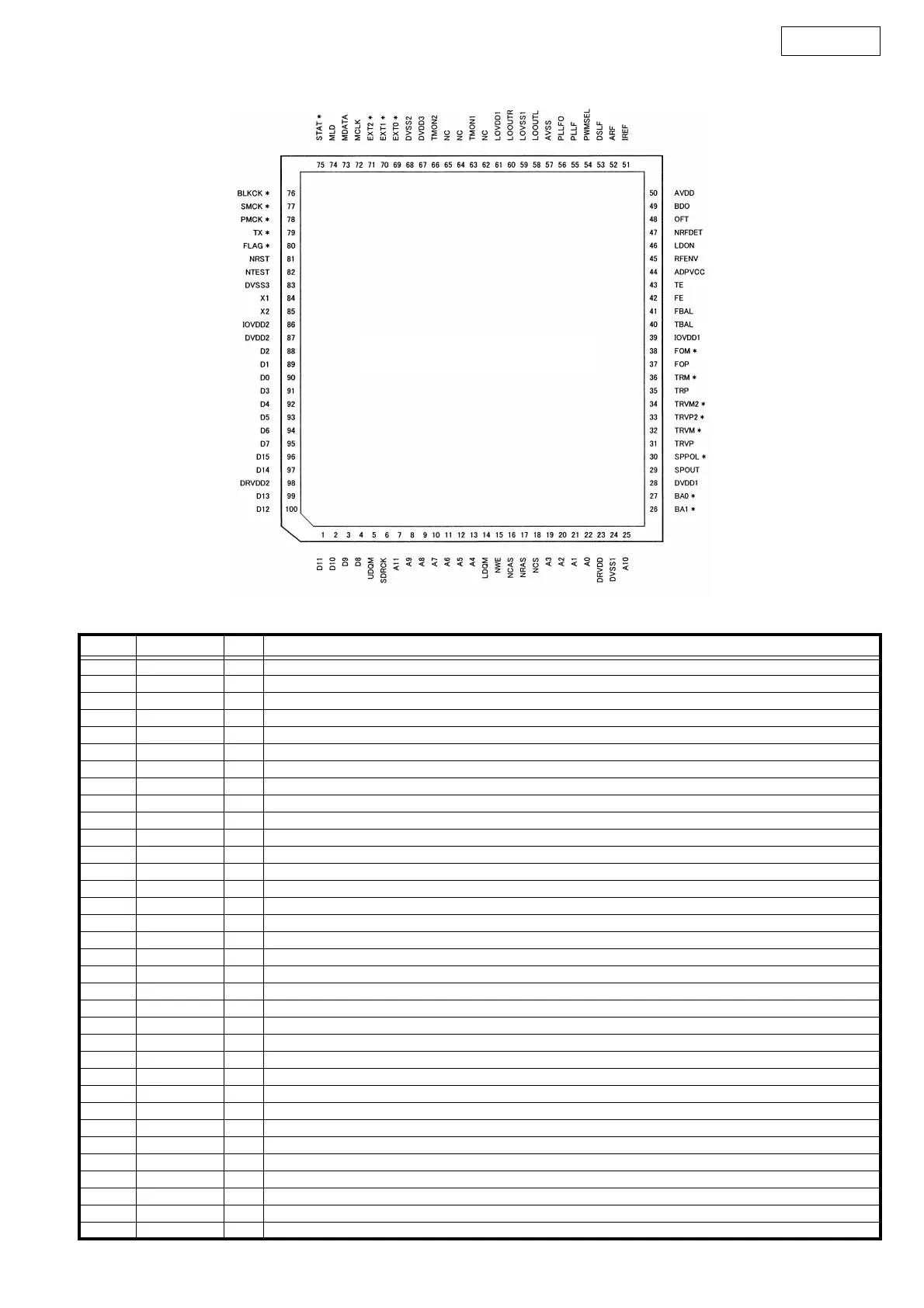
MN6627933 (IC101,201)
MN6627933 Terminal Function
Pin No. Pin Name I/O Function
1 D11 I/O SDRAM data signal I/O 11
2 D10 I/O SDRAM data signal I/O 10
3 D9 I/O SDRAM data signal I/O 9
4 D8 I/O SDRAM data signal I/O 8
5 UDQM O SDRAM higher rank byte data mask signal output
6 SDRCK O SDRAM clock signal output
7 A11 O SDRAM address signal output 11
8 A9 O SDRAM address signal output 9
9 A8 O SDRAM address signal output 8
10 A7 O SDRAM address signal output 7
11 A6 O SDRAM address signal output 6
12 A5 O SDRAM address signal output 5
13 A4 O SDRAM address signal output 4
14 LDQM O SDRAM lower rank byte data mask signal output
15 NEW O SDRAM write enable signal output
16 NCAS O SDRAM CAS control signal output
17 NRAS O SDRAM RAS control signal output
18 NCS O SDRAM chip select signal output
19 A3 O SDRAM address signal output 3
20 A2 O SDRAM address signal output 2
21 A1 O SDRAM address signal output 1
22 A0 O SDRAM address signal output 0
23 DRVDD1 I Power supply 1 for SDRAM interface I/O
24 DVSS1 I GND 1 for digital circuits
25 A10 O SDRAM address signal output 10
26 *BA1 O SDRAM bank selection signal output 1
27 *BA0 O SDRAM bank selection signal output 0
28 DVDD1 I Power supply 1 for inside digital circuits
29 SPOUT O Spindle drive signal output (absolute value)
30 *SPPOL O Spindle drive signal output (polarity)
31 TRVP O Traverse drive signal output (positive polarity)
32 *TRVM O Traverse drive signal output (negative polarity)
33 *TRVP2 O Traverse drive signal output 2 (positive polarity)
34 *TRVM2 O Traverse drive signal output 2 (negative polarity)
MN
6627933
CN