49
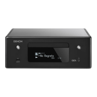
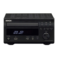
RCD-CX1
Terminal Function
Pin No. Pin Name Function
1 AGND Analog ground for control chip power supply.
2 VSS Negative power supply for control chip (-5V).
3 THM Thermal Monitor
Error signal of open collector output “L” for two conditions.
1. Over temperature limitation.
2. Over temperature warning. By connecting to the ENA pin, thermal shutdown is set.
4 ENA Bi-direction input/output.
The input “H” enables to start switching and the input “L” disables.
Input is including hysteresis for glitch free enable of the system.
When the protection circuit detects the over voltage condition, the open collector output turns on.
5NC
6 OCM Over Current Monitor
Error signal of open collector output “L” for two conditions.
1. Over current limitation.
2. For monitoring the state of control and average voltage across the zobel resistor in case of of-limit
conditions.
7 DCG This high impedance output generates a current in case of over voltage condition on the power stage
voltage (VD/VS).
This current is designed to turn-on a set of discharge transistors.
8 VSCK This high impedance input for monitoring negative power stage.
This monitoring controls the soft clipping circuit and the over voltage shutdown.
9 AGND Analog ground for control chip power supply.
10 VDCK This high impedance input for monitoring positive power stage.
This monitoring controls the soft clipping circuit and the over voltage shutdown.
11 VSS Negative power supply for control chip (-5V).
12 AGND Analog ground for control chip power supply.
13 NC
14 AGND2 Input reference for channel 2.
This is true inverting low impedance (1kohm) input for avoiding ground loop noise.
15 IN2+ High impedance audio input for channel 2.
This input is non-inverting.
16 AGND1 Input reference for channel 1.
This is true non-inverting low impedance (2kohm) input for avoiding ground loop noise.
17 IN1- High impedance audio input for channel 1.
This input is inverting.
18 NC
19 TEST Test terminal connect to VSS.
20 VSS Negative power supply for control chip (-5V).
21 AGND Analog ground for control chip power supply.
22 VDD Positive power supply for control chip (+5V).
23 FB1 Feedback for global loop of channel 1.
24 NC
25 ZB1 For estimating the power dissipation in the zobel resister,
this input is sensing the zobel voltage via a resistive network of channel 1.
26 VDR1 Positive supply for driver chip of channel 1 with respect to VS1; (VS1+10V).
27 VD1 Positive supply for power stage of channel 1.
28 VD1 Positive supply for power stage of channel 1.
29 VS1 Negative supply for power stage of channel 1.
30 VS1 Negative supply for power stage of channel 1.
31 PWM1 PWM output of channel 1.
32 PWMFB1 Feedback for inner loop of channel 1.
33 SUB Substrate of IMST.
34 VS Negative supply for power stage.
35 VDR2 Positive supply for driver chip of channel 2 with respect to VS2;(VS2+10V).
36 VD2 Positive supply for power stage of channel 2.
37 VD2 Positive supply for power stage of channel 2.
38 VS2 Negative supply for power stage of channel 2.
39 VS2 Negative supply for power stage of channel 2.
40 PWM2 PWM output of channel 2.
41 PWMFB2 Feedback for inner loop of channel 2.
42 ZB2 For estimating the power dissipation in the zobel resister,
this input is sensing the zobel voltage via a resistive network of channel 2.
43 NC
44 FB2 Feedback for global loop of channel 2.

 Loading...