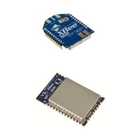
XBee® Wi-Fi RF Modules
© 2013 Digi International, Inc. 101
AT
Command
Name and Description
Parameter
Range
Default
D5 DIO5 Configuration. Select/Read function for DIO5
0 = Disabled
1 = Associated LED
3 = Digital input
4 = Digital output,
default low
5 = Digital output,
default high
1
D8 DIO8 Configuration. Select/Read function for DIO8
1 = SleepRq
3 = Digital input,
monitored
4 = Digital output,
default low
5 = Digital output,
default high
1
D9 DIO9 Configuration. Select/Read function for DIO9
0 = Disabled
1 = On/Sleep
indicator
3 = Digital input,
monitored
4 = Digital output,
default low
5 = Digital output,
default high
1
LT
Assoc LED Blink Time. Set/Read the Associate LED blink time. If the Associate LED
functionality is enabled (D5 command), this value determines the on and off blink
times for the LED when the module has joined a network. If LT=0, the default blink
rate of 250ms will be used. For all other LT values, LT is measured in 10ms.
0, 0x14 - 0xFF (200 -
2550 ms)
0
PR
Pull-up Resistor. Set/read the bit field that configures the internal resistor status for
the I/O lines. "1" specifies the resistor is enabled. "0" specifies no resistor. The PD
command specifies whether the resistor is pull-up or pull-down. Pin numbers are
listed with the TH module pin first, followed by the SMT module pin (e.g. pin 11/24
indicates pin 11 on the through-hole module and pin 24 on the surface mount
module.)
Bits:
0 – DIO4 (Pin 11/24) 10 – DIO12 (Pin 4/5)
1 – DIO3 / AD3 (Pin 17/30) 11 – DIO10 / PWM0 (Pin 6/7)
2 – DIO2 /AD2 (Pin 18/31) 12 – DIO11/PWM1 (Pin 7/8)
3 – DIO1/AD1 (Pin 19/32) 13 – DIO7 / CTS (Pin 12/25)
4 – DIO0 / AD0 (Pin 20/33) 14 – DIO13/DOUT (pin2/3)
5 – DIO6 / RTS (Pin 16/29) 15 – DIO15 (pin NA/17)
6 – DIO8 / nDTR / Sleep Request (Pin 9/10) 16 – DIO16 (Pin NA/16)
7 – DIN / Config (Pin 3/4) 17 – DIO17 (Pin NA/15)
8 – DIO5 / Associate (Pin 15/28) 18 – DIO18 (Pin NA/14)
9 – DIO9 / On/Sleep (Pin 13/26) 19 – DIO19 (Pin NA/12)
0 - 0x7FFF 0x7FFF
PD
. Set/Read resistor direction for the corresponding bits set in PR (1 =
pull up, 0 = pull down). If the bit is not set in PR, then PD is unused.
0 – 0x7FFF on TH
0 – 0xFFFFF on SMT
0x7FFF on TH
0xFFFFF on SMT
DS
Set/Read the output drive strength (output amperes) for DIO lines.
Bits are mapped the same as the PR and PD commands. If the bit is set, the drive
strength is 6mA . Otherwise, it is 2mA.
0 – 0x7FFF on TH
0 – 0xFFFFF on SMT
0
AV
Analog Voltage Reference. Set/Read the analog voltage reference. This specifies
the volts for an analog reading of 0x03ff, where a reading of 0x200 indicates a
voltage input that is half of VREF. VREF may be one of these two values:
0 – 1.25Volts
0-1 1
M0
PWM0 Duty cycle. Sets the duty cycle of PWM0 for P0=2, where a value of 0x200 is a
0 – 0x03FF
0
M1
PWM1 Duty cycle. Sets the duty cycle of PWM1 for P1=2, where a value of 0x200 is a
0 – 0x03FF
0
* indicates that the option is available on the TH module, but not the SMT module
** indicates that the command is available on the SMT module, but not the TH module

 Loading...