RX
-
8025
SA
/
NB
Page - 2 ETM10E-04
3. Description of Pins
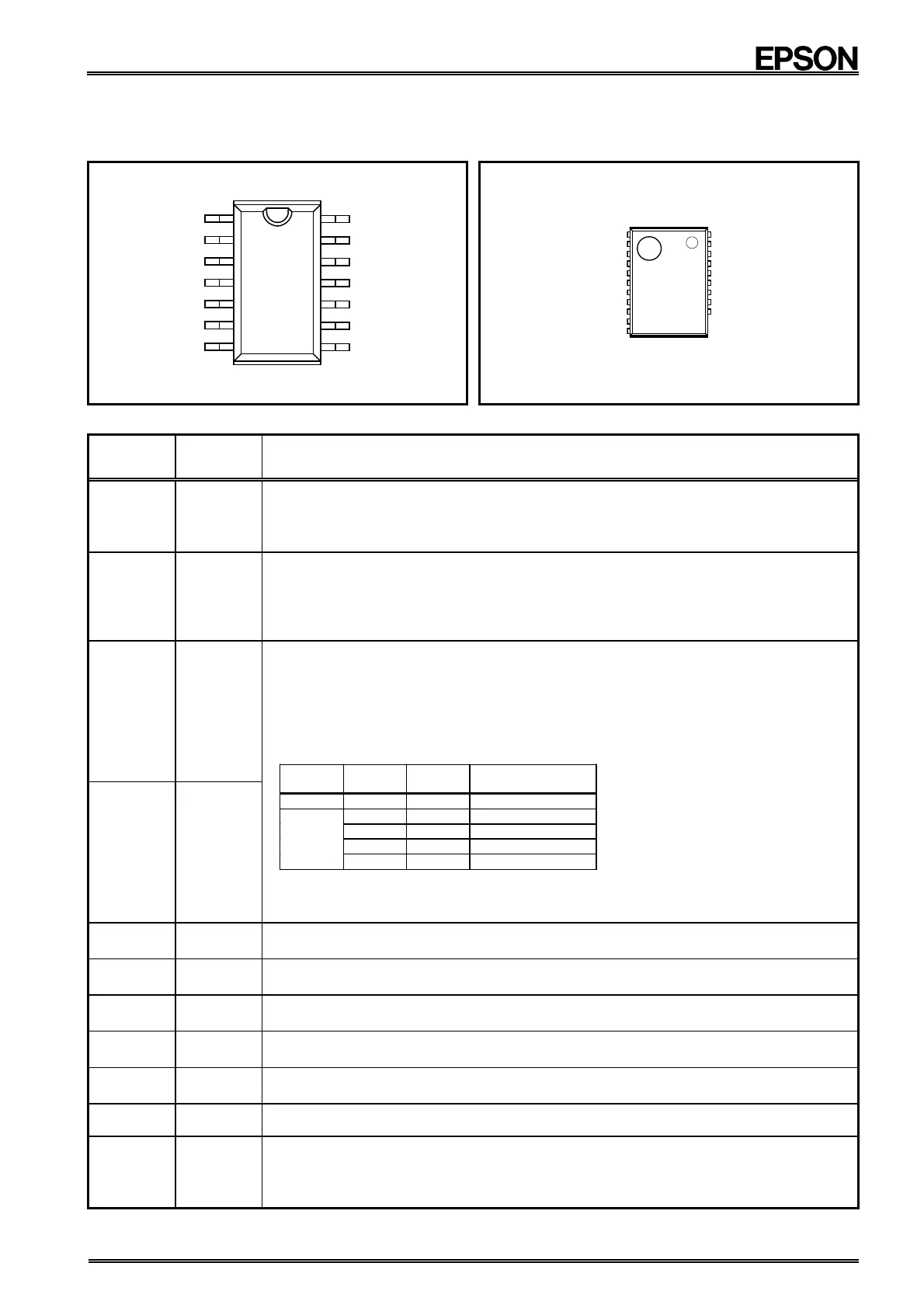
3.1. Pin Layout
RX - 8025 SA
N.C.
N.C.
SCL
SDA
FOUT
/ INTB
N.C.
GND
TEST
/ INTA
VDD
N.C.
FOE
N.C.
SOP - 14pin
RX - 8025 NB
FOE 22. N.C.
VDD 21. N.C.
(GND)
20. N.C.
TEST 19. N.C.
FOUT 18. N.C.
SCL 17. N.C.
SDA 16. N.C.
/ INTB 15. N.C.
GND 14. N.C.
/ INTA (13)
−
N.C.
# 1
# 11
# 22
(#12)
(12)
−
SON - 22pin
3.2. Pin Functions
Signal
name
I / O Function
SCL I
This is the serial clock input pin for I
2
C communications. Data input and output across the
SDA pin is synchronized with this pin's clock signal.
Up to 5.5 V can be used for this input, regardless of the power supply voltage.
SDA I/O
This pin's signal is used for input and output of address, data, and ACK bits, synchronized
with the serial clock used for I
2
C communications.
The SDA pin is an N-ch open drain pin during output. Be sure to connect a suitable pull-up
resistance relative to the signal line capacity.
FOUT O
FOUT terminal is 32.768 kHz clock output terminal (C-MOS) that output control is possible.
FOE terminal is the input terminal controlling the output of FOUT pin with /CLEN1 and
/CLEN2 bit.
The output of FOUT terminal stops when /CLEN1bit and /CLEN2 bit both sets to "1".
FOUT output stops when FOE is Low or OPEN. Status of FOUT output stopped is " L ".
∗The logic table.
FOE
input
/CLEN1
bit
/CLEN2
bit
FOUT
output
L
Χ
Χ
OFF (
"
L
"
)
0 0 32.768 kHz
0 1 32.768 kHz
1 0 32.768 kHz
H
1 1
OFF (
"
L
"
)
' Χ ' Don't care.
FOE terminal had pull-down resistor built-in and input voltage is possible regardless of
power supply voltage to 5.5 V.
FOE I
/INTA O
This interrupt output A pin is an N-ch open drain output.
It outputs alarm interrupts (Alarm_D) and periodic interrupts.
/INTB O
This interrupt output B pin is an N-ch open drain output.
It outputs alarm interrupts (Alarm_W).
TEST
−
This pin is used by the manufacturer for testing. Do not connect externally.
V
DD
−
This pin is connected to a positive power supply.
GND
−
This pin is connected to a ground.
(GND)
−
This pin has the same voltage level as GND. Do not connect externally.
N.C.
−
This pin is not connected to the internal IC.
However, note with caution that the RX-8025NB's N.C. pins (pins 14 to 22) are interconnected
via the internal frame.
Leave N.C. pins open or connect them to GND or V
DD
.
Note: Be sure to connect a bypass capacitor rated at least 0.1 µF between V
DD
and GND.