RX
-
8025
SA
/
NB
Page - 20 ETM10E-04
8.7. The various detection Functions
The detection functions include detection of power-on resets, oscillation stops, and supply voltage drops, as well as
reporting of detection results in corresponding bits of the address Fh (Control 2) register.
The status of the power supply, oscillation circuit, and clock can be confirmed by checking these results.
∗ Note with caution that detection functions may not operate correctly when power flickers occur.
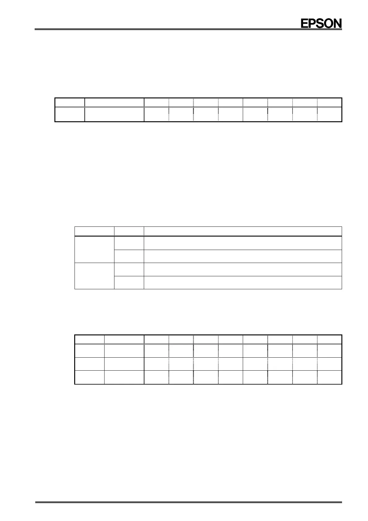
8.6.1. Related register
Address
Function bit 7 bit 6 bit 5 bit 4 bit 3 bit 2 bit 1 bit 0
F Control 2
VDSL
VDET
/ XST
PON
/CLEN1
CTFG WAFG DAFG
(Default)
(0) (0)
(−
−−
−)
(1)
( 0 ) (0) (0) (0)
∗1) The default value is the value that is read (or is set internally) after the PON bit has been set to "1," such as after powering up from 0 V or
recovering from a supply voltage drop.
∗2) '"−" indicates undefined status.
8.7.1. Power-on reset detection
This function detects when a power-on reset occurs. When a power-on reset is detected, the PON bit value becomes
"1".
A reset is detected when a power-on from 0 V has occurred, including when the power-on reset from 0 V occurred
due to a supply voltage drop.
1) PON bit
This bit indicates the detection results when a power-on reset has occurred.
The power-on reset function operates when a power-on from 0 V has occurred, including when a power-on reset
from 0 V occurred due to a supply voltage drop. When this function operates, the PON bit value becomes "1".
The /XST and VDET bits can be used in combination to determine the valid/invalid status of the clock and
calendar data.
PON Data Description
Write
0
Clears PON bit to zero and sets up for next detection operation
1
The writes "1" are invalid.
Read
0
Power-on reset was not detected
1
Power-on reset was detected
(result is that bit value is held until cleared to zero)
∗ Default
∗ When PON = "1" the clock precision adjustment register, Control register 1, and Control register 2 (except
for PON and /XST) are reset and cleared to "0". This stops (sets Hi-Z for) output from the /INTA and
/INTB pins.
2) Status of other bits when power-on reset is detected
• Internal initialization status during a power-on reset
Address
Function bit 7 bit 6 bit 5 bit 4 bit 3 bit 2 bit 1 bit 0
7 Digital Offset
0 F6 F5 F4 F3 F2 F1 F0
(Default) (0) (0) (0) (0) (0) (0) (0) (0)
E Control 1 WALE
DALE
/12, 24
/CLEN2
TEST
CT2 CT1 CT0
(Default) (0) (0) (0)
( 0 ) ( 0 )
(0) (0) (0)
F Control 2 VDSL
VDET
/ XST
PON /CLEN1
CTFG
WAFG
DAFG
(Default) (0) (0)
(−)
( 1 ) ( 0 )
(0) (0) (0)
∗1) The default value is the value that is read (or is set internally) after the PON bit has been set to "1," such
as after powering up from 0 V or recovering from a supply voltage drop.
∗2) " −" indicates undefined status.
∗3) At this point, all other register bits are undefined, so be sure to perform a reset before using the module.
Also, be sure to avoid entering incorrect date and time data, as clock operations are not guaranteed
when the time data is incorrect.