RX
-
8025
SA
/
NB
Page - 4 ETM10E-04
7.1.2. DC electrical characteristics (2)
* Unless otherwise specified, GND
= 0 V, V
DD
= 3 V, Ta = −40 °C to +85 °C
Item
Condition Min. Typ. Max. Unit
Input current with pull-down
resistance
I
FOE
FOE pin, V
I
= 5.5 V
0.3 1.0
µA
Output current when OFF
I
OZ
SDA, /INTA, and /INTB pins
V
O
= 5.5 V or GND, V
DD
= 5.5 V
−1
1
µA
Power
supply
detection
voltage
High-voltage
mode
V
DETH
V
DD
pin, Ta = −30 to +70 °C
1.90 2.10 2.30 V
Low-voltage
mode
V
DETL
V
DD
pin, Ta = −30 to +70 °C
1.15 1.30 1.45 V
7.2. AC Electrical Characteristics
∗ Unless otherwise specified: GND = 0 V, V
DD
= 1.7 V to 5.5 V, Ta = −40 °C to +85 °C
∗ Input conditions: V
IH
= 0.8 × V
DD
, V
IL
= 0.2 × V
DD
, V
OH
= 0.8 × V
DD
, V
OL
= 0.2 ×V
DD
, CL = 50 pF
Item Symbol
Condition
Min. Typ. Max. Unit
SCL clock frequency f
SCL
400 kHz
SCL clock low time t
LOW
1.3
µs
SCL clock higt time t
HIGH
0.6
µs
Start condition hold time t
HD;STA
0.6
µs
Stop condition setup time t
SU;STO
0.6
µs
Start condition setup time t
SU;STA
0.6
µs
Recovery time from stop condition
to start condition
t
RCV
62
µs
Data setup time
tSU:DAT
200 ns
Data hold time
tHD;DAT
0 ns
SDA “L” stable time after falling of SCL
tPL;DAT
0.9
µs
SDA off stable time after falling of SCL
tPZ;DAT
0.9
µs
Rising time of SCL and SDA (input)
tR
300 ns
Falling time of SCL and SDA (input)
tF
300 ns
Spike width that can be removed
with input filter
tSP
50 ns
Caution: When accessing this device, all communication from transmitting the start condition to transmitting the stop
condition after access should be completed within 0.5 seconds.
If such communication requires 0.5 to 1.0 second or longer, the I
2
C bus interface is reset by the internal bus
timeout function. Please see also 8.8.3. Starting and stopping I
2
C bus communications.
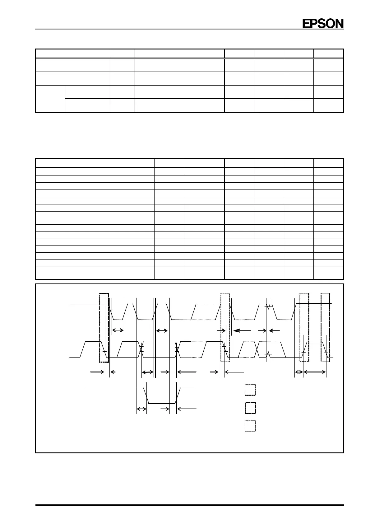
SDA(OUT)
SCL
S
Sr
P
t
PZ;DAT
t
HIGH
t
t
HD;STA
t
SP
t
SU;STO
t
LOW
t
SU;STA
SDA(IN)
t
HD;STA
t
PL;DAT
Sr
P
STOP condition
S
START Condition
Re-start condition
t
HD;DAT
S
t
RCV