Reproduction forbidden without Fibocom Wireless Inc. written authorization - All Rights Reserved.
L831-EAU-01 Hardware User Manual Page
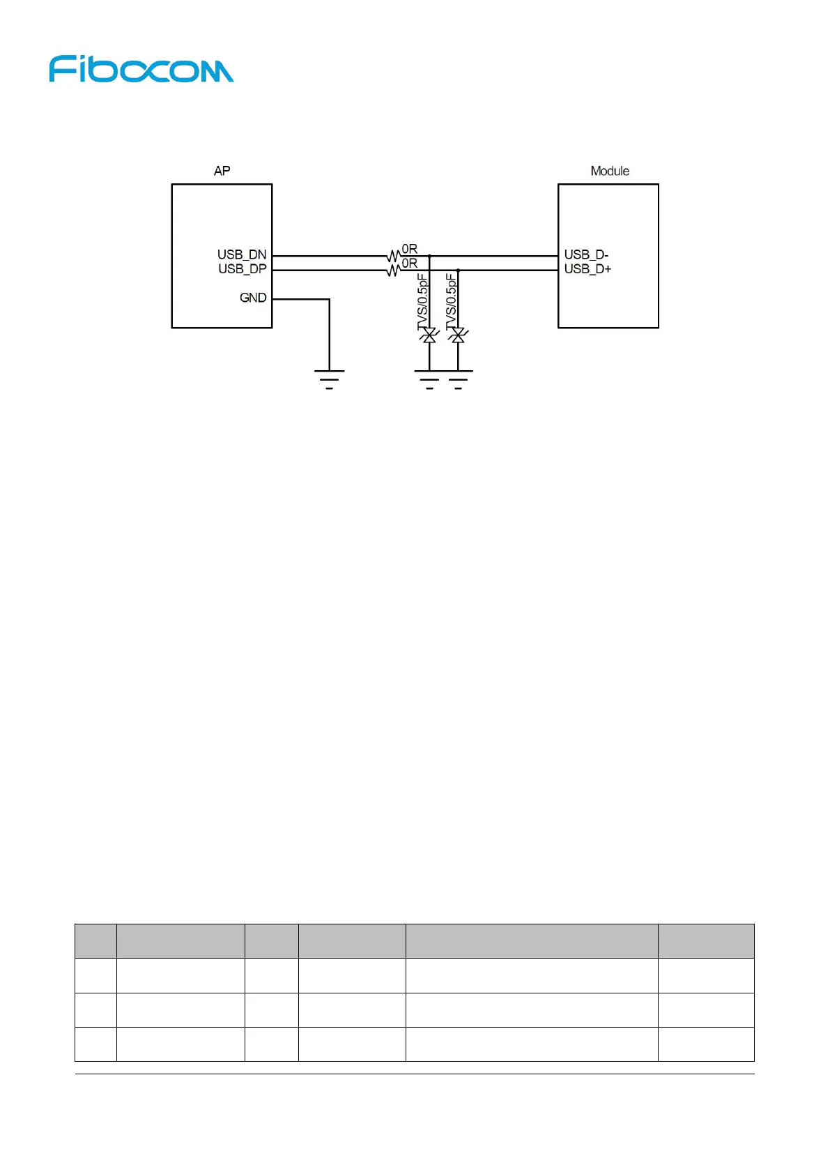
3.4.2 USB2.0 Interface Application
The reference circuit is shown in Figure 3-14:
Figure3- 14 Reference Circuit for USB 2.0 Interface
Since the module supports USB 2.0 High-Speed, it is required to use TVS diodes with equivalent
capacitance of 1pF or smaller ones on the USB_D-/D+ differential signal lines, it is recommended to use
USB_D- and USB_D+ are high speed differential signal lines with the maximum transfer rate of 480 Mbit/s,
so the following rules shall be followed carefully in the case of PCB layout:
USB_D- and USB_D+ signal lines should have the differential impedance of 90 ohms.
USB_D- and USB_D+ signal lines should be parallel and have the equal length, the right angle
routing should be avoided.
USB_D- and USB_D+ signal lines should be routed on the layer that is adjacent to the ground
layer, and wrapped with GND vertically and horizontally.
The L831-EAU module has a built-in USIM card interface, which supports 1.8V and 3V SIM cards.
The USIM pins description as shown in the following table: