Do you have a question about the Fibocom L830-EB and is the answer not in the manual?
Provides an overview of the document's purpose and scope for developers.
Lists the industry standards the product design complies with.
References other documentation relevant to the L830 module.
Introduces the L830 as an integrated 4G cellular module using M.2 interface.
Details key technical specifications including bands, data transmission, and physical characteristics.
Illustrates the peripheral applications and module integration.
Presents the internal hardware architecture including baseband and RF functions.
Describes the standard M.2 Key-B interface and its 75 pins.
Provides a detailed pinout map for the M.2 interface.
Defines each pin of the M.2 interface, including I/O, type, and description.
Details the power supply requirements and design considerations for the module.
Defines the 1.8V and 3.3V logic level parameters for the module.
Lists the power consumption values under different operating modes.
Explains the control signals for power on/off and reset operations.
Describes the circuits and methods for module start-up.
Details the software and hardware methods for shutting down the module.
Explains how to reset the module and the recommended circuit design.
Covers the USB 2.0 interface compatibility and definition.
Describes the USIM card interface, pins, and circuit design.
Explains the SIM card hot-plugging function and its configuration.
Details the status indicator signals like LED#1 and WOWWAN#.
Covers interrupt signals such as W_DISABLE1# and Body SAR detection.
Explains the I2S and PCM modes for digital audio interface.
Describes the I2C master interface for external slave devices.
Details the clock interface for outputting a 26MHz clock signal.
Explains the configuration pins for the M.2 module type.
Mentions interfaces not supported by the module.
Details the RF connectors, functionality, characteristics, and dimensions.
Lists the operating frequency bands supported by the module.
Specifies the transmitting power for each supported band.
Provides the receiver sensitivity values for various bands.
States the GNSS support status for the L830-EB-11 module.
Outlines the antenna design requirements and considerations for the module.
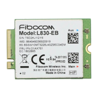
Shows the visual appearance and front/back of the L830 module.
Provides the detailed physical dimensions of the L830 module.
Specifies the M.2 interface model type and pin assignments.
Details recommended storage conditions and storage life.
Describes the packing methods used for the L830 module.
| Category | Computer Hardware |
|---|---|
| Manufacturer | Fibocom |
| Model | L830-EB |
| Form Factor | M.2 |
| Operating Temperature | -10°C to +55°C |
| LTE Bands | B1/B3/B5/B7/B8/B20 |
| 3G Bands | B1/B5/B8 |
| Data Rate | LTE Cat4: 150Mbps DL / 50Mbps UL |
| Interface | PCIe, USB 2.0 |
| Operating Voltage | 3.135V to 4.4V |