Chapter 4: 21
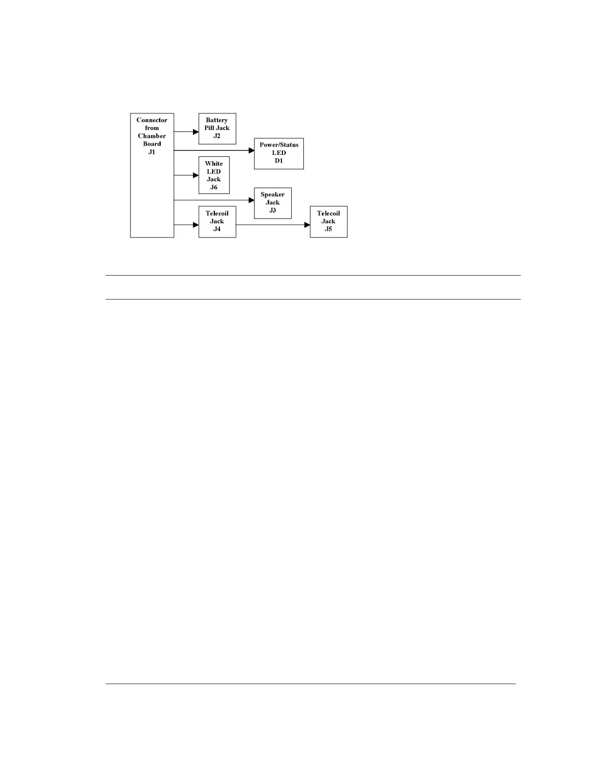
4.3.6 Breakout Board Block Diagram
4.4 Circuits Detailed Description
All the circuits on each board are described here. The Chamber and Connector
boards can be configured more than one way. On these boards, some of the circuits
are left off in each configuration.
4.4.1 Source Circuits Signal Flow
4.4.1.1 SBC: The source signal originates at the CODEC on the SBC.
4.4.1.2 Daughterboard schematic (061-0171-0x)
OUTGOING SIGNAL:
Page 3: The two channels arrive on J3 pins 5 and 1. A sample of the analog
ground on the SBC is taken from J3 pin 8. U3 and U4 and associated
circuits then re-reference the ground of the source signal from the SBC
ground to the SPKREF ground which connects to system MECCA on page
5. The two source signals are named “SOURCE_A” and “SOURCE_B” and
then sent to the connectorboard via J5 pins 6 and 7. The SPI Buss from
U1-A on page 1 is send to the Connectorboard via J5 pins 15, 16, and
17(SPIMOSI, SPICLK, SPICSL).
Page 1: The SPI Buss originates on U1-A pins 46, 40, and 39(SPICLK, SPIMOSI,
SPICSL).
RETURNING CURRENT:
Page 3: The source return currents (SRETA and SRETB) arrive on J5 pins 5 and 8.
Page 5: They are then sent to the current measurement circuit comprised of U16
and associated resistors. The currents cause a voltage drop across R71