Preliminary
30(45)
Prepared Document Number
Manfred Ortmann
Approved Checked Date Revision Storage
2009-10-05 PA 4.2 Mycable01
Pin Signal Function
120
VCC18 1.8 V, regulated on XXSvideo for DDR2
SDRAM
Tab. 2-4: Pin assignment of connector X401, I/O signals side
2.2.4 Configuration
R201 - R204
R301 - R306
R401 – R408
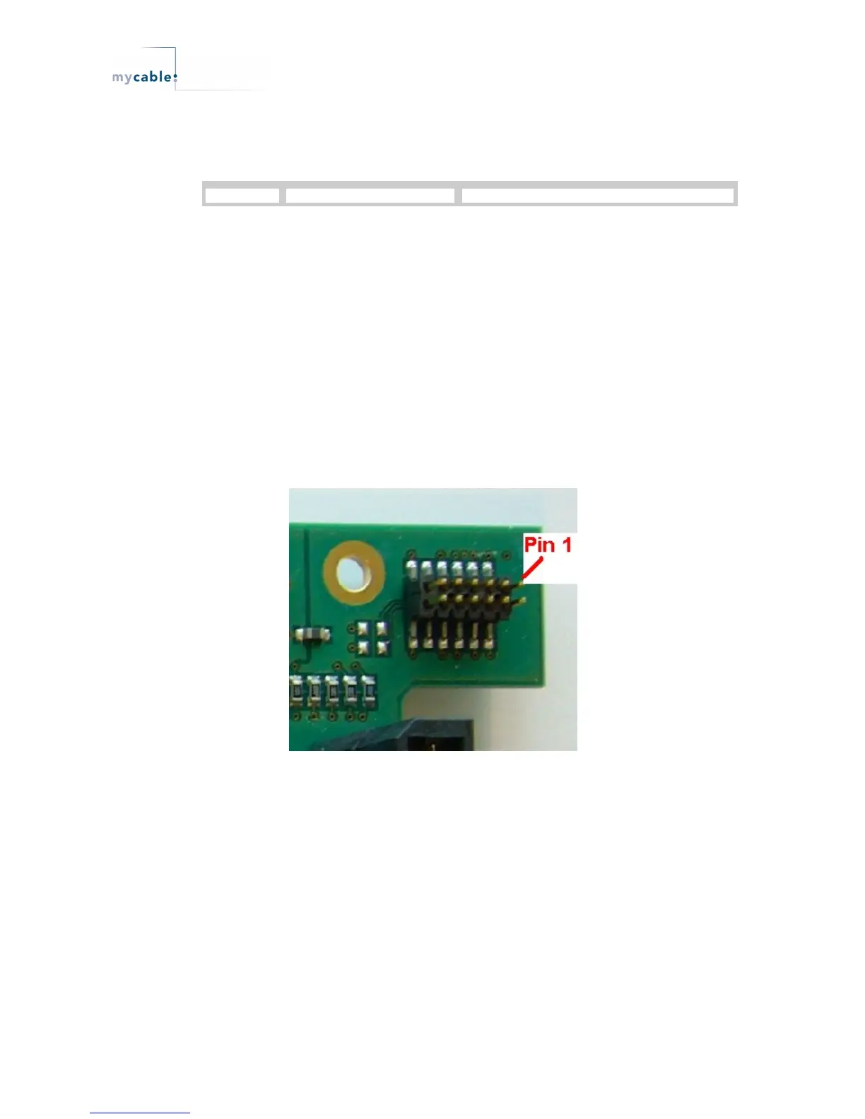
2.2.5 ADC Interface
Pic. 2-8: ADC interface
The pins of the ADC interface from the JADE-D on the XXSvideo-D are available at connector
X805, FTSH-106-01-L-DV from Samtec.
At AD_VR0 and AD_VR1 are capacitors with 100 nF to Ground connected.
Resistors ( R840 – R845 ) with connection to AD_VRH0, AD_VRL0, AD_VRH1 and AD_VRL1
can be populated. As default these resistors are not populated. Details see schematic.