Revision C 170 Series Monitor 5-19
2000947-004
Theory of Operation: Main Board Theory of Operation
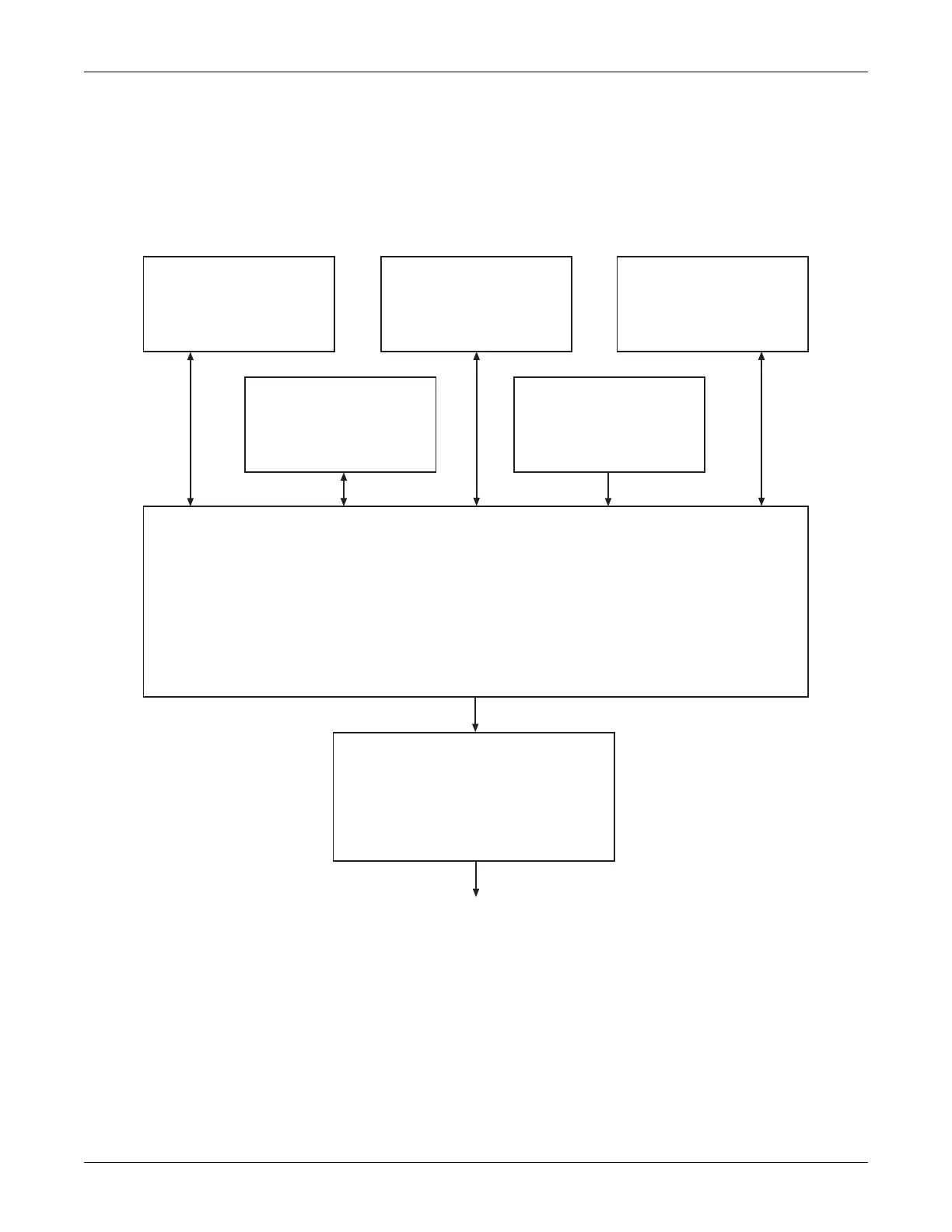
Processing Block
The processing block consists of the processor, system memory, battery RAM (with
real time clock), and address decoder PAL. Figure 5-11 provides a block diagram of
the processing block.
Figure 5-11. Processing Circuitry Block Diagram
SH3 Processor
to peripheral devices
System Boot Flash Memory
(128k x 8)
System SDRAM Memory
(1M x 32 standard)
System Control/Address Decoder PAL
Address decoding
Recorder control latch and head
protection timer
SPI chip select and clock control
Recorder serial interface
System Flash Memory
512k x 32 standard
512k x 32 optional
Battery RAM with
Real Time Clock
(8k x 8)
12.288 MHz Crystal