Table of Figures
Figure 1: P64x version evolution 7
Figure 2: Functional overview 11
Figure 3: Hardware architecture 30
Figure 4: Exploded view of IED 31
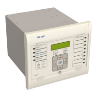
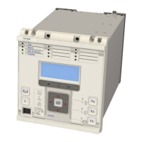
Figure 5: Front panel (60TE) 34
Figure 6: HMI panel 35
Figure 7: Rear view of populated case 38
Figure 8: Terminal block types 39
Figure 9: Rear connection to terminal block 40
Figure 10: Main processor board 41
Figure 11: Power supply board 42
Figure 12: Power supply assembly 43
Figure 13: Power supply terminals 44
Figure 14: Watchdog contact terminals 45
Figure 15: Rear serial port terminals 46
Figure 16: Input module - 1 transformer board 46
Figure 17: Input module schematic 47
Figure 18: Frequency response 48
Figure 19: Transformer board 49
Figure 20: Input board 50
Figure 21: Standard output relay board - 8 contacts 51
Figure 22: IRIG-B board 52
Figure 23: Fibre optic board 53
Figure 24: Rear communication board 54
Figure 25: Ethernet board 54
Figure 26: Redundant Ethernet board 56
Figure 27: RTD board 58
Figure 28: RTD board 59
Figure 29: High Break relay output board 61
Figure 30: High Break contact operation 62
Figure 31: Software Architecture 66
Figure 32: Frequency Response (indicative only) 72
Figure 33: Navigating the HMI 79
Figure 34: Default display navigation 81
Figure 35: Compensation using biased differential characteristic 101
Figure 36: Transformer winding connections - part 1 103
Figure 37: Transformer winding connections - part 2 104
Figure 38: Magnetising inrush phenomenon 105