Cinterion
®
ALAS5 Hardware Interface Overview
2.2 GSM/UMTS/LTE Antenna Interface
32
ALAS5_HIO_v00.030a 2019-04-01
Confidential / Preliminary
Page 27 of 50
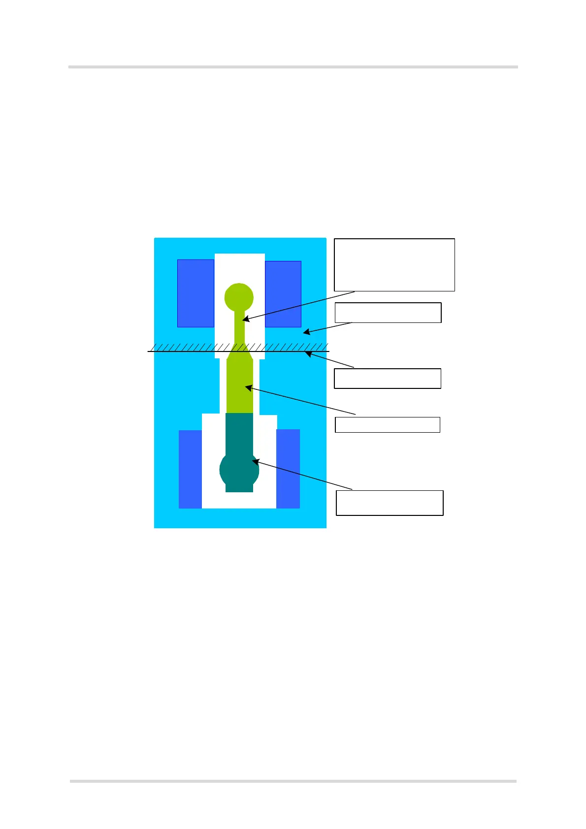
2.2.2.2 Routing Examples
Interface to RF Connector
Figure 10 shows a sample connection of a module‘s antenna pad at the bottom layer of the
module PCB with an application PCB‘s coaxial antenna connector. Line impedance depends
on line width, but also on other PCB characteristics like dielectric, height and layer gap. The
sample stripline width of 0.40mm is recommended for an application with a PCB layer stack
resembling the one of the ALAS5 evaluation board. For different layer stacks the stripline width
will have to follow stripline routing rules, avoiding 90 degree corners and using the shortest dis-
tance to the PCB’s coaxial antenna connector.
Figure 10: Routing to application‘s RF connector
e.g.
ANT_
MAIN
G N D
G N D
Edge of module PCB
Stripline (50 ohms) on top
layer of evaluation board from
antenna pad to module edge
Width = 0.40 mm
E.g., U.FL antenna
connector
50 ohms microstrip line
G N D G N D
Ground connection

 Loading...