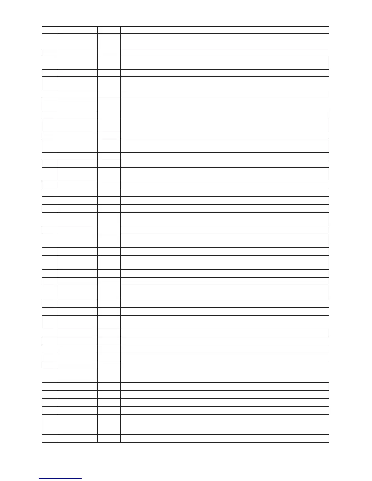
No . Pin Name I/O Function
40 NC -
No Co nnect pin
No internal bonding . Th is pin should be opened.
41 RO UT 3 O DA C3 Rc h An alog Ou tput Pi n
42 NC -
No Co nnect pin
No internal bonding . Th is pin should be opened.
43 LO UT 2 OD AC 2 Lc h An alog Ou tput Pin
44 NC -
No Co nnect pin
No internal bonding . Th is pin should be opened.
45 RO UT 2 O DA C2 Rc h An alog Ou tput Pi n
46 NC -
No Co nnect pin
No in ternal bondin g. This pin should be opened.
47 LO UT 1 OD AC 1 Lc h An alog Ou tput Pin
48 NC -
No Co nnect pin
No internal bonding . Th is pin should be opened.
49 RO UT 1 O DA C1 Rc h An alog Ou tput Pi n
50 NC -
No Co nnect pin
No internal bonding . Th is pin should be opened.
51 LI N IL ch An alog Input Pin
52 RI N I Rc h An alog Input Pin
53 VC OM -
Co mmon Vo ltage Ou tput Pin
2.2F capacitor should be connected to AV SS externally.
54 VR EF H-
Po siti ve Vo ltage Reference Input Pin , AVDD
55 A VDD - An alog Power Supply Pin, 4.5V~ 5.5V
56 AV SS -
An alog Gr ound Pin, 0V
57 RX 0 I R eceiver Chan nel 0 Pi n (Internal biased pin. Internally biased at PV DD/ 2)
58 NC -
No Co nnect pin
No internal bonding. This pin should be connected to PV SS.
59 RX 1 I R eceiver Chan nel 1 Pi n (Internal biased pin. Internally biased at PV DD/ 2)
60 TE ST 1I
Test 1 Pi n
Th is pin should be connected to PV SS.
61 RX 2 I R eceiver Chan nel 2 Pi n (Internal biased pin. Internally biased at PV DD/ 2)
62 NC -
No Co nnect pin
No internal bonding. This pin should be connected to PV SS.
63 RX 3 I R eceiver Chan nel 3 Pi n (Internal biased pin. Internally biased at PV DD/ 2)
64 PV SS -P LL Gr ound pin
65 R -
Ex ternal Re sistor Pi n
12k +/-1% resistor should be connected to PV SS externally.
66 P VDD -
PL L Po wer supply Pin, 4.5V~ 5.5V
67 RX 4 I R eceiver Chan nel 4 Pi n (Internal biased pin. Internally biased at PV DD/ 2)
68 TE ST 2I
Test 2 Pi n
Th is pin should be connected to PV SS.
69 RX 5 I R eceiver Chan nel 5 Pi n (Internal biased pin. Internally biased at PV DD/ 2)
70 C AD0 I
Ch ip A ddress 0 Pi n (ADC/ DAC part)
71 RX 6 I R eceiver Chan nel 6 Pi n (Internal biased pin. Internally biased at PV DD/ 2)
72 C AD1 I
Ch ip A ddress 1 Pi n (ADC/ DAC part)
73 RX 7I R eceiver Chan nel 7 Pi n (Internal biased pin. Internally biased at PV DD/ 2)
74 I2CI
Co ntrol Mo de Select Pin.
"L": 4-wi re Seri al, "H": I
2
C Bu s
75 D AUX2 I Au xili ary Au dio Data Input Pin (D IR/DIT part)
76 VI NI V-bit Input Pin for Transmitter Ou tput
77 MC LK I
Ma ster Cl ock Input Pin
78 TX0 OT ransmit Ch annel (Through Data) Ou tput 0 Pi n
79 TX 1 O
Transmit Ch annel Ou tput1 pin
Wh en TX bit = "0", Transmit Ch annel (Through Data) Ou tput 1 Pi n.
Wh en TX bit = "1", Transmit Ch annel (DAUX2 Data) Ou tput Pi n (Def ault).
80 IN T0 OI nterrupt 0 Pin
No te : A ll in put pins except internal biased pins and internal pull -down pin should not be left floating.
 Loading...