PRELIMINARY W9864G6JH
Publica
tion Release Date: Jan. 25, 2010
- 5 - Revision P01
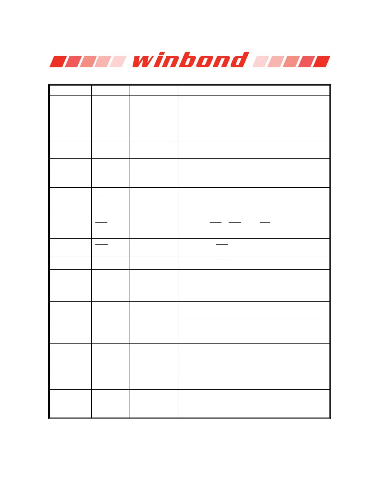
5. PIN DESCRIPTION
PIN NUMBER
PIN NAME
FUNCTION DESCRIPTION
23 ~ 26, 22,
29 ~35
A0−A11
Address
Multiplexed pins for row and column address.
Row address: A0−A11. Column address: A0−A7.
A10 is sampled during a precharge command to
determine if all banks are to be precharged or bank
selected by BS0, BS1.
20, 21
BS0, BS1 Bank Select
Select bank to activate during row address latch time,
or bank to read/write during address latch time.
11, 13, 42, 44,
45, 47, 48, 50,
51, 53
DQ0−DQ15
Data
Input/ Output
Multiplexed pins for data output and input.
19
Chip Select
Disable or enable the command decoder. When
command decoder is disabled, new command is
ignored and previous operation continues.
18
Row Address
Strobe
Command input. When sampled at the rising edge of
the clock
,
and
to be executed.
17
Column
Address Strobe
Referred to
16
Write Enable
Referred to
39, 15
UDQM
LDQM
Input/output
mask
The output buffer is placed at Hi-Z (with latency of 2)
when DQM is sampled high in read cycle. In write
cycle, sampling DQM high will block the write
operation with zero latency.
38 CLK Clock Inputs
System clock used to sample inputs on the rising
edge of clock.
37 CKE Clock Enable
CKE controls the clock activation and deactivation.
When CKE is low, Power Down mode, Suspend
mode, or Self Refresh mode is entered.
1, 14, 27 VDD Power Power for input buffers and logic circuit inside DRAM.
28, 41, 54 VSS Ground
Ground for input buffers and logic circuit inside
DRAM.
3, 9, 43, 49 VDDQ
Power for I/O
buffer
Separated power from VDD, to improve DQ noise
immunity.
6, 12, 46, 52
VSSQ
Ground for I/O
buffer
Separated ground from VSS, to improve DQ noise
immunity.
36, 40 NC No Connection
No connection.
 Loading...