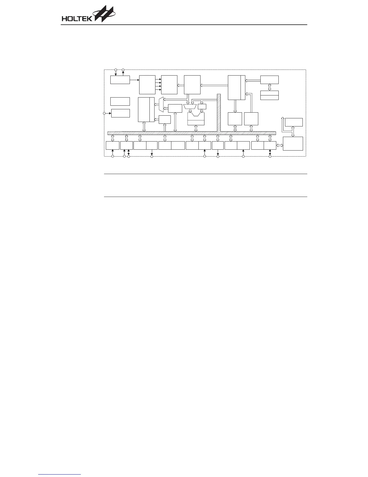
Block Diagram
The following block diagram illustrates the main functional blocks of the A/D Type microcontroller
series of devices.
Note
This block diagram represents the OTP devices, for the mask device there is no Device Pro
-
gramming Circuitry. The HT46R47/HT46C47 does not contain an I
2
C interface. The Bank Pointer
only exists in the HT46R24/HT46C24.
6
A/D Type MCU
T i m i n g
G e n e r a t o r
S y s t e m R C /
X ' t a l O s c i l l a t o r
I n s t r u c t i o n
D e c o d e r
I n s t r u c t i o n
R e g i s t e r
W D T
O s c i l l a t o r
D a t a
M e m o r y
A d d r e s s D e c o d e r
M e m o r y
P o i n t e r
M U X
A C C
C o n f i g .
R e g i s t e r
W a t c h d o g
T i m e r
R e s e t &
L V R
C o n f i g .
R e g i s t e r
T i m e r ( s ) /
C o u n t e r
L o o k - u p
T a b l e
R e g i s t e r
P r o g r a m
M e m o r y
A d d r e s s D e c o d e r
S t a c k
S t a c k P o i n t e r
P r o g r a m
C o u n t e r
L o o k - u p
T a b l e
P o i n t e r
C o n f i g .
R e g i s t e r
I / O
P o r t s
D e v i c e
P r o g r a m m i n g
C i r c u i t r y
C o n f i g u r a t i o n
O p t i o n
T o P r o g r a m
M e m o r y
A L U
S h i f t e r
M
U
X
C o n f i g .
R e g i s t e r
I n t e r r u p t
C i r c u i t
P F D
A / D
C o n v e r t e r
C o n f i g .
R e g i s t e r
P W M
I
2
C
B a n k
P o i n t e r