Note 1. Each pin on PA can be programmed through a configuration option to have a wake-up function.
2. Individual pins on PA and PB can be selected to have pull-high resistors. However, individual
pins on Port C, Port D and Port F cannot be selected to have pull-high resistors. If the pull-high
configuration is chosen for a particular PC, PD or PF port, then all input pins on the
corresponding port will have pull-high resistors connected.
3. The pin description table is based on the 48-pin package. Due to packaging limitations some
I/O pins may not exist on the 28-pin package. The TMR0 external pin is not available on the
28-pin package. The TMR1 pin is available on the 28-pin package as the pin-shared
PD1/PWM1/TMR1.
Absolute Maximum Ratings
Supply Voltage.............................................................................................V
SS
-0.3V to V
SS
+6.0V
Input Voltage ...............................................................................................V
SS
-0.3V to V
DD
+0.3V
Storage Temperature.............................................................................................-50°Cto125°C
Operating Temperature............................................................................................-40°Cto85°C
These are stress ratings only. Stresses exceeding the range specified under Absolute Maximum
Ratings may cause substantial damage to the device. Functional operation of this device at other
conditions beyond those listed in the specification is not implied and prolonged exposure to ex
-
treme conditions may affect device reliability.
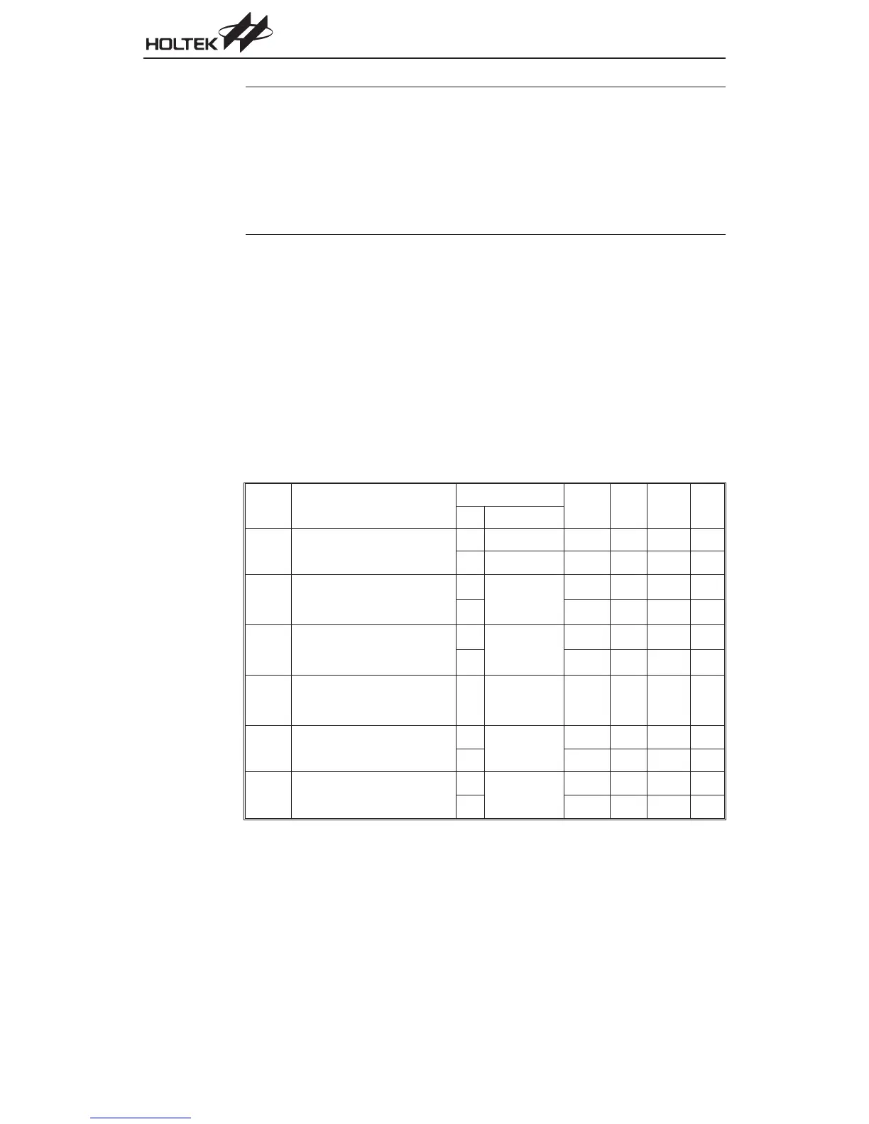
D.C. Characteristics
Ta=25°C
Symbol Parameter
Test Conditions
Min. Typ. Max. Unit
V
DD
Conditions
V
DD
Operating Voltage
¾
f
SYS
=4MHz
2.2
¾
5.5 V
¾
f
SYS
=8MHz
3.3
¾
5.5 V
I
DD1
Operating Current
(Crystal OSC)
3V No load,
f
SYS
=4MHz
ADC off
¾
0.6 1.5 mA
5V
¾
24mA
I
DD2
Operating Current
(RC OSC)
3V No load,
f
SYS
=4MHz
ADC off
¾
0.8 1.5 mA
5V
¾
2.5 4 mA
I
DD3
Operating Current
(Crystal OSC, RC OSC)
5V
No load,
f
SYS
=8MHz
ADC off
¾
48mA
I
STB1
Standby Current
(WDT Enabled)
3V
No load,
system HALT
¾¾
5
mA
5V
¾¾
10
mA
I
STB2
Standby Current
(WDT and A/D Disabled)
3V
No load,
system HALT
¾¾
1
mA
5V
¾¾
2
mA
A/D Type MCU
12
 Loading...