rupt control register, and if the interrupts are enabled, an appropriate internal interrupt signal will
be generated. This A/D internal interrupt signal will direct the program flow to the associated A/D in
-
ternal interrupt address for processing. If the A/D internal interrupt is disabled, the microcontroller
can be used to poll the EOCB bit in the ADCR register to check whether it has been cleared as an
alternative method of detecting the end of an A/D conversion cycle.
A/D Converter Clock Source Register - ACSR
The clock source for the A/D converter, which originates from the system clock f
SYS
, is first divided
by a division ratio, the value of which is determined by the ADCS1 and ADCS0 bits in the ACSR
register.
Although the A/D clock source is determined by the system clock f
SYS
, and by bits ADCS1 and
ADCS0, there are some limitations on the maximum A/D clock source speed that can be selected.
As the minimum value of permissible A/D clock period t
AD
is 1ms, for system clock speeds in ex
-
cess of 2MHz, the ADCS1 and ADCS0 bits should not be set to ²00². Doing so will give A/D clock
periods that are less than 1ms which may result in inaccurate A/D conversion values. Refer to the
following table for examples, where values marked with an asterisk * are not permissible as they
are less than the specified minimum A/D Clock Period.
f
SYS
A/D Clock Period (t
AD
)
ADCS1, ADCS0=00
(f
SYS
/2)
ADCS1, ADCS0=01
(f
SYS
/8)
ADCS1, ADCS0=10
(f
SYS
/32)
ADCS1, ADCS0=11
1MHz
2ms8ms32ms
Undefined
2MHz
1ms4ms16ms
Undefined
4MHz 500ns*
2ms8ms
Undefined
8MHz 250ns*
1ms4ms
Undefined
A/D Clock Period Examples
A/D Input Pins
All of the A/D analog input pins are pin-shared with the I/O pins on Port B. The PCR2~PCR0 bits in
the ADCR register, not configuration options, determine whether the input pins are setup as nor
-
mal Port B input/output pins or whether they are setup as analog inputs. In this way, pins can be
changed under program control to change their function from normal I/O operation to analog in
-
puts and vice versa. Pull-high resistors, which are setup through configuration options, apply to
the input pins only when they are used as normal I/O pins, if setup as A/D inputs the pull-high resis
-
tors will be automatically disconnected. Note that it is not necessary to first setup the A/D pin as an
Chapter 1 Hardware Structure
49
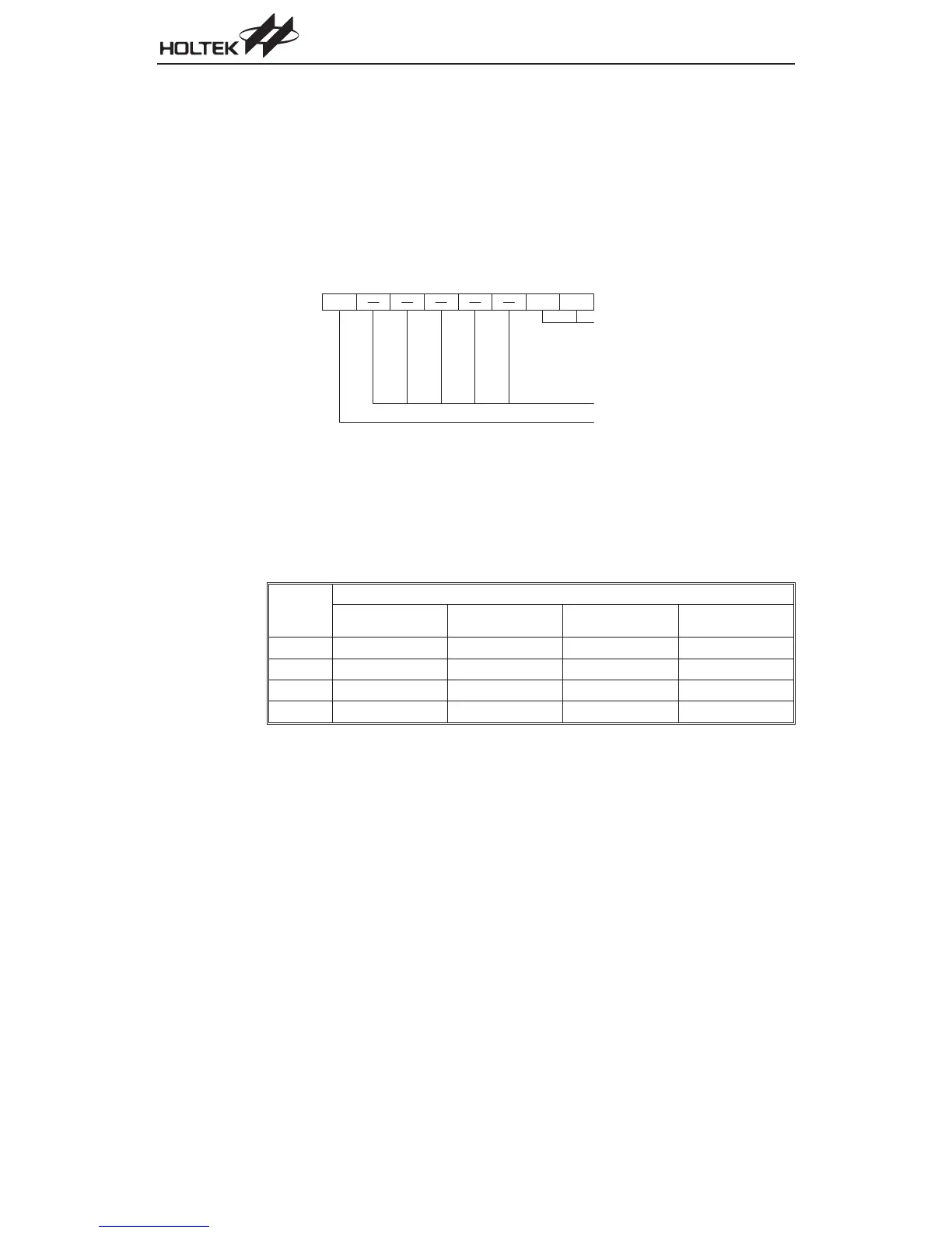
A C S R R e g i s t e r
S e l e c t A / D c o n v e r t e r c l o c k s o u r c e
b 7 b 0
T E S T
A D C S 1 A D C S 0
A D C S 1
0
0
1
1
A D C S 0
0
1
0
1
: s y s t e m c l o c k / 2
: s y s t e m c l o c k / 8
: s y s t e m c l o c k / 3 2
: u n d e f i n e d
N o t i m p l e m e n t e d , r e a d a s " 0 "
F o r t e s t m o d e u s e o n l y