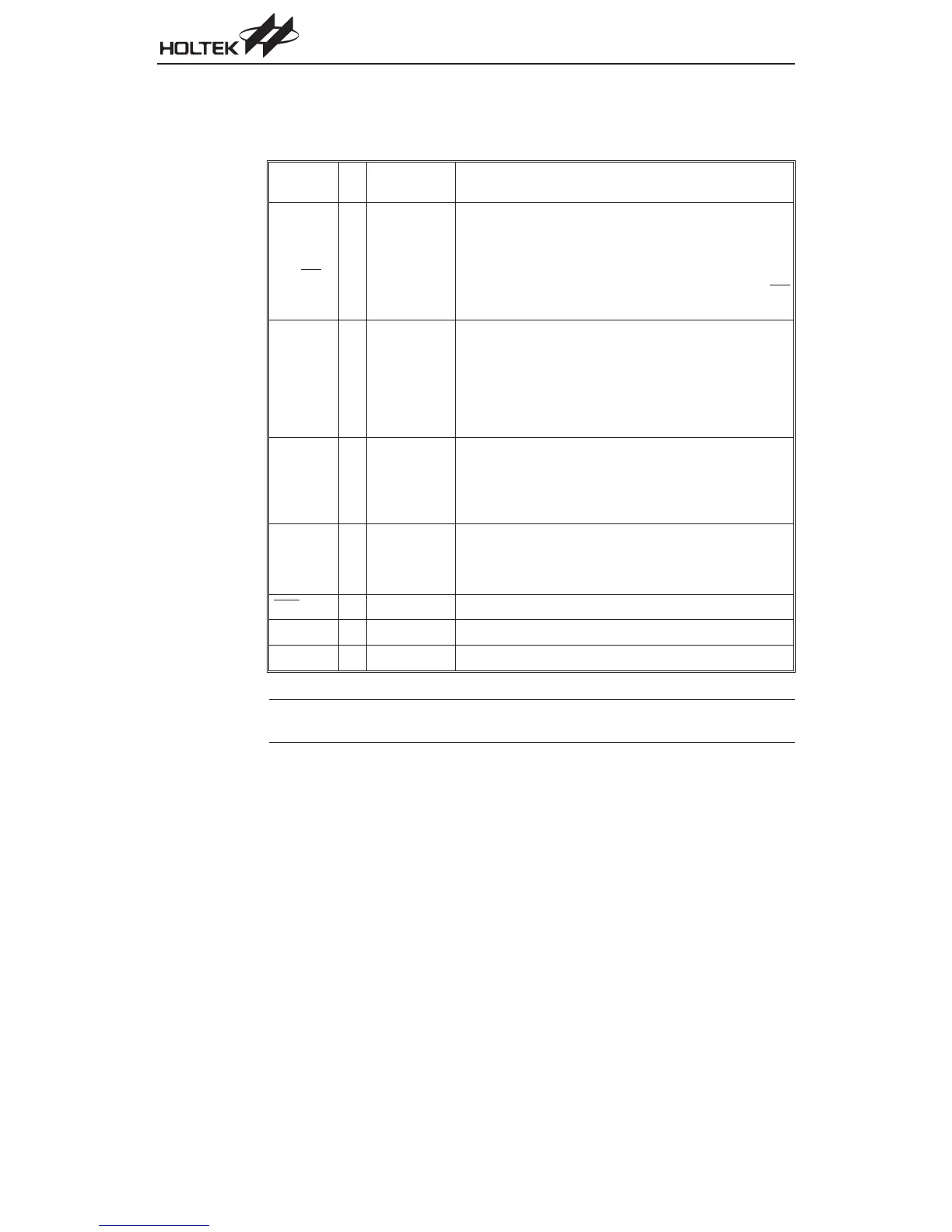
Pin Description
HT46R47/HT46C47
Pin Name I/O
Configuration
Option
Description
PA0~PA2
PA3/PFD
PA4/TMR
PA5/INT
PA6~PA7
I/O
Pull-high
Wake-up
PA3 or
PFD
Bidirectional 8-bit input/output port. Each individual bit on this
port can be configured as a wake-up input by a configuration
option. Software instructions determine if the pin is a CMOS
output or Schmitt Trigger input. A configuration option deter
-
mines which bits on the port have pull-high resistors. Pins
PA3, PA4 and PA5 are pin-shared with PFD, TMR and INT
respectively.
PB0/AN0
PB1/AN1
PB2/AN2
PB3/AN3
I/O Pull-high
Bidirectional 4-bit input/output port. Software instructions de
-
termine if the pin is a CMOS output or Schmitt Trigger input. A
configuration option determines which bits on the port have
pull-high resistors. PB is pin-shared with the A/D input pins.
The A/D inputs are selected via software instructions. Once
selected as an A/D input, the I/O function and pull-high resis
-
tor functions are disabled automatically.
PD0/PWM I/O
Pull-high
I/O or
PWM
Bidirectional 1-bit input/output port. Software instructions de
-
termine if the pin is a CMOS output or Schmitt Trigger input. A
configuration option determines if this pin has a pull-high re
-
sistor. The PWM output is pin-shared with pin PD0 selected
via configuration option.
OSC1
OSC2
I
O
Crystal or RC
OSC1, OSC2 are connected to an external RC network or ex-
ternal crystal (determined by configuration option) for the in-
ternal system clock. For external RC system clock operation,
OSC2 is an output pin for 1/4 system clock.
RES I
¾
Schmitt Trigger reset input. Active low.
VDD
¾¾
Positive power supply
VSS
¾¾
Negative power supply, ground
Note 1. Each pin on PA can be programmed through a configuration option to have a wake-up function.
2. Each pin on each port can be individually configured to have a pull-high resistor.
8
A/D Type MCU