Because the TBLH register is a read-only register and cannot be restored, care should be taken to
ensure its protection if both the main routine and Interrupt Service Routine use table read instruc
-
tions. If using the table read instructions, the Interrupt Service Routines may change the value of
the TBLH and subsequently cause errors if used again by the main routine. As a rule it is recom
-
mended that simultaneous use of the table read instructions should be avoided. However, in situa
-
tions where simultaneous use cannot be avoided, the interrupts should be disabled prior to the
execution of any main routine table-read instructions. Note that all table related instructions re
-
quire two instruction cycles to complete their operation.
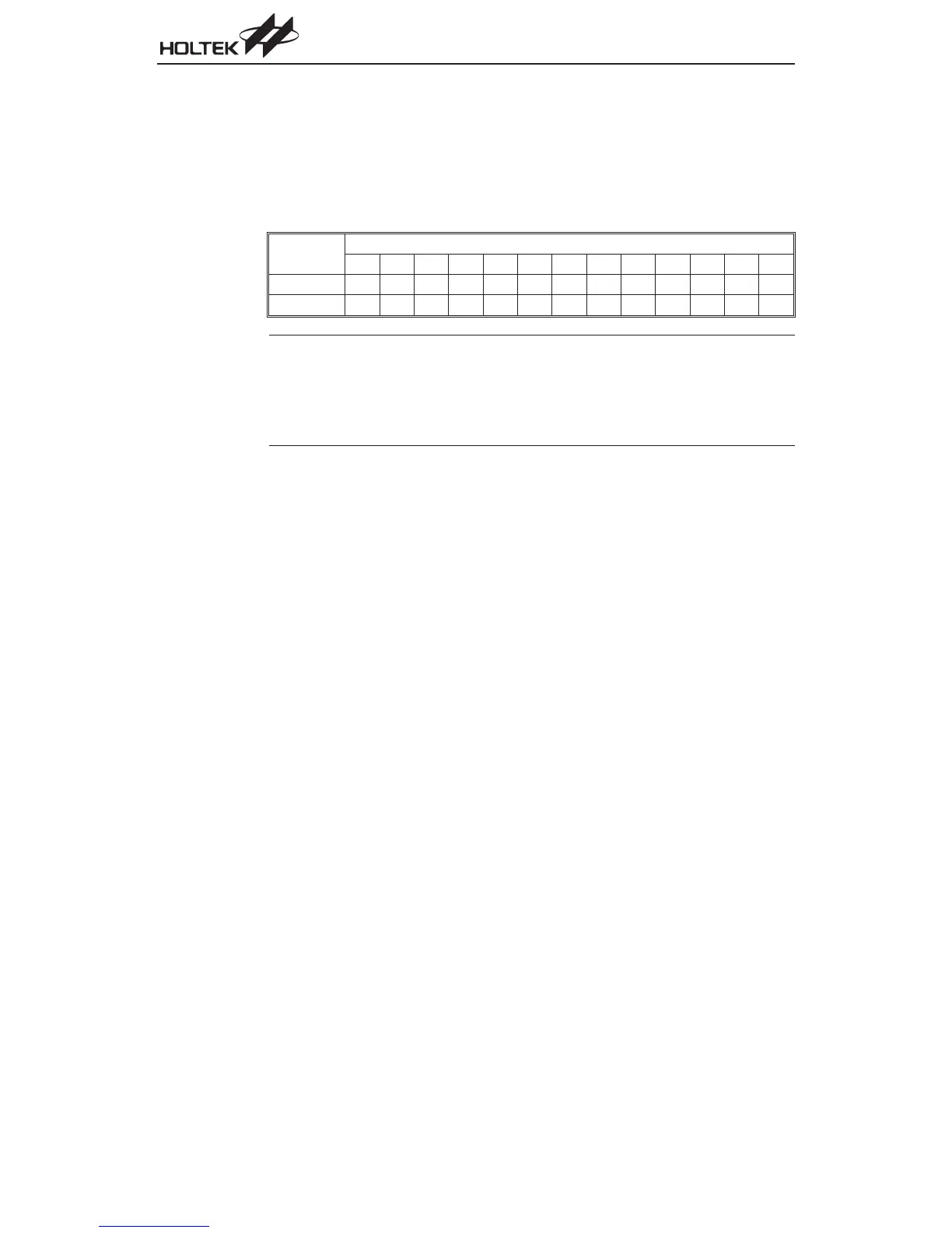
Instruction
Table Location Bits
b12 b11 b10 b9 b8 b7 b6 b5 b4 b3 b2 b1 b0
TABRDC
[m] PC12 PC11 PC10 PC9 PC8 @7 @6 @5 @4 @3 @2 @1 @0
TABRDL
[m]11111@7@6@5@4@3@2@1@0
Note 1. PC12~PC8: Current Program Counter bits
2. @7~@0: Table Pointer TBLP bits
3. For the HT46R24/HT46C24, the Table address location is 13 bits, i.e. from b12~b0.
4. For the HT46R23/HT46C23, the Table address location is 12 bits, i.e. from b11~b0.
5. For the HT46R47/HT46C47 and HT46R22/HT46C22, the Table address location is 11 bits, i.e.
from b10~b0.
Data Memory
The Data Memory is a volatile area of 8-bit wide RAM internal memory and is the location where
temporary information is stored. Divided into two sections, the first of these is an area of RAM
where special function registers are located. These registers have fixed locations and are neces-
sary for correct operation of the device. Many of these registers can be read from and written to di-
rectly under program control, however, some remain protected from user manipulation. The
second area of Data Memory is reserved for general purpose use. All locations within this area are
read and write accessible under program control.
Organization
The two sections of Data Memory, the Special Purpose and General Purpose Data Memory are lo-
cated at consecutive locations. All are implemented in RAM and are 8 bits wide but the length of
each memory section is dictated by the type of microcontroller chosen. The start address of the
Data Memory for all devices is the address 00H. The last Data Memory address is 7FH for the
HT46R47/HT46C47 and HT46R22/HT46C22 devices, and FFH for the HT46R23/HT46C23 and
HT46R24/HT46C24 devices. Registers which are common to all microcontrollers, such as ACC,
PCL etc., have the same Data Memory address.
22
A/D Type MCU