HT46R22/HT46C22
Pin Name I/O
Configuration
Option
Description
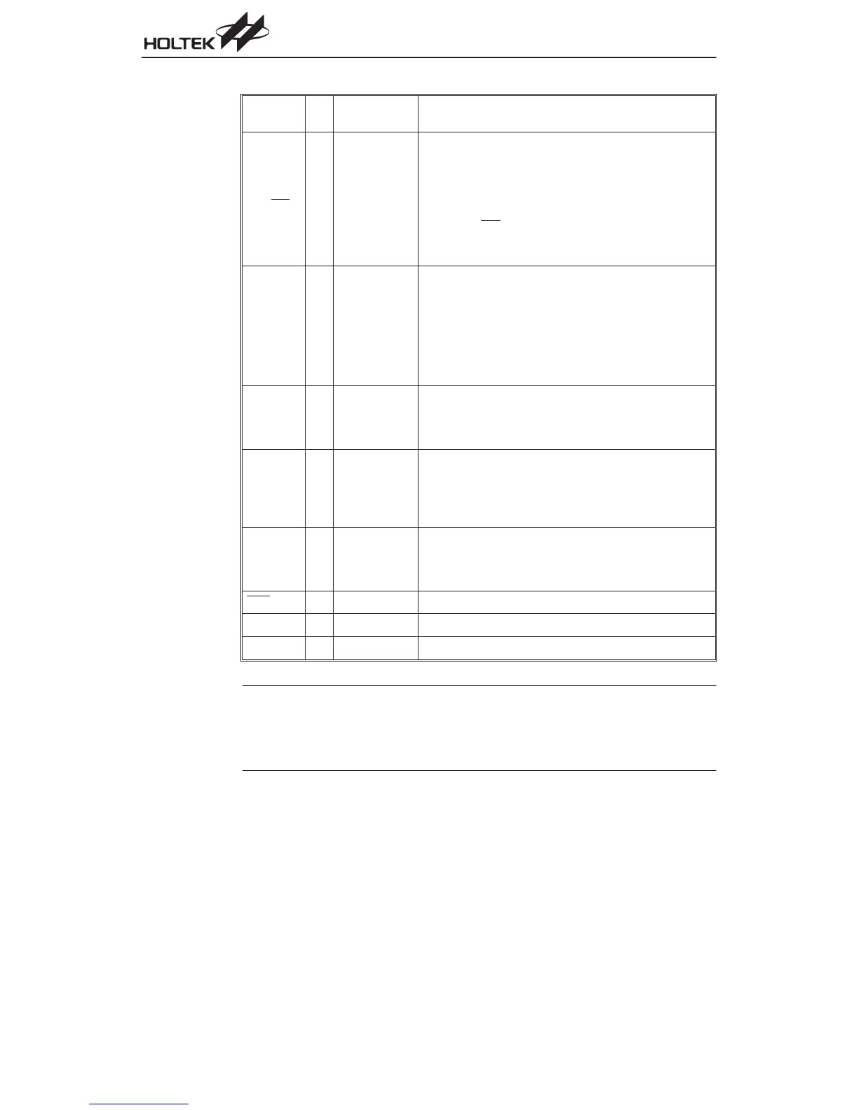
PA0~PA2
PA3/PFD
PA4/TMR
PA5/INT
PA6/SDA
PA7/SCL
I/O
Pull-high
Wake-up
PA3 or PFD
PA6/PA7 or
SDA/SCL
Bidirectional 8-bit input/output port. Each individual bit on
this port can be configured as a wake-up input by a configu
-
ration option. Software instructions determine if the pin is a
CMOS output or Schmitt Trigger input. A configuration op
-
tion determines which bits on the port have pull-high resis
-
tors. Pins PA3, PA4 and PA5 are pin-shared with PFD,
TMR and INT
respectively. Pins PA6 and PA7 are
pin-shared with SDA and SCL respectively and are used to
implement the I
2
C bus function.
PB0/AN0
PB1/AN1
PB2/AN2
PB3/AN3
PB4/AN4
PB5/AN5
PB6/AN6
PB7/AN7
I/O Pull-high
Bidirectional 8-bit input/output port. Software instructions
determine if the pin is a CMOS output or Schmitt Trigger in
-
put. A configuration option determines if all pins on the port
have pull-high resistors. PB is pin-shared with the A/D input
pins. The A/D inputs are selected via software instructions.
Once selected as an A/D input, the I/O function and
pull-high resistor functions are disabled automatically.
PC0~PC1 I/O Pull-high
Bidirectional 2-bit input/output port. Software instructions
determine if the pin is a CMOS output or Schmitt Trigger in
-
put. A configuration option determines if both pins on this
port have pull-high resistors.
PD0/PWM I/O
Pull-high
I/O or PWM
Bidirectional 1-bit input/output port. Software instructions
determine if the pin is a CMOS output or Schmitt Trigger in
-
put. A configuration option determines if this pin has a
pull-high resistor. The PWM output is pin-shared with pin
PD0 selected via configuration option.
OSC1
OSC2
I
O
Crystal or RC
OSC1, OSC2 are connected to an external RC network or
external crystal (determined by configuration option) for the
internal system clock. For external RC system clock opera-
tion, OSC2 is an output pin for 1/4 system clock.
RES I
¾
Schmitt Trigger reset input. Active low.
VDD
¾¾
Positive power supply
VSS
¾¾
Negative power supply, ground
Note 1. Each pin on PA can be programmed through a configuration option to have a wake-up function.
2. Individual pins on PA can be selected to have a pull-high resistors. However, individual pins on
Port B and Port C cannot be selected to have pull-high resistors. If the pull-high configuration
is chosen for a particular PB or PC port, then all input pins on this port will be connected to
pull-high resistors.
Chapter 1 Hardware Structure
9