Rev. 2.50 102 June 22, 2017 Rev. 2.50 103 June 22, 2017
HT66F20/HT66F30/HT66F40/HT66F50/HT66F60
HT66FU30/HT66FU40/HT66FU50/HT66FU60
A/D Flash MCU with EEPROM
HT66F20/HT66F30/HT66F40/HT66F50/HT66F60
HT66FU30/HT66FU40/HT66FU50/HT66FU60
A/D Flash MCU with EEPROM
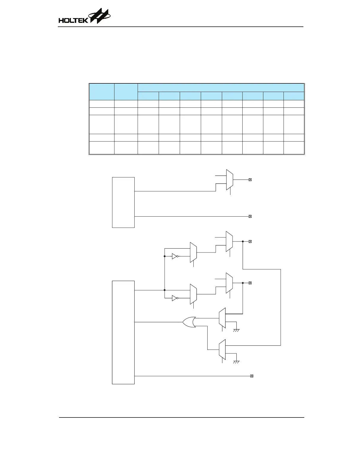
TM Input/Output Pin Control Registers
SelectingtohaveaTMinput/outputorwhethertoretainitsothersharedfunction,isimplemented
usingoneortworegisters,withasinglebitineachregistercorrespondingtoaTMinput/outputpin.
SettingthebithighwillsetupthecorrespondingpinasaTMinput/output,ifresettozerothepin
willretainitsoriginalotherfunction.
Registers Device
Bit
7 6 5 4 3 2 1 0
TMPC0 HT66F20 — —
T1CP1 T1CP0 — — — T0CP0
TMPC0 HT66F30
T1ACP0 — T1BCP1 T1BCP0 — — T0CP1 T0CP0
TMPC0
HT66F40
HT66F50
HT66F60
T1ACP0 T1BCP2 T1BCP1 T1BCP0 — — T0CP1 T0CP0
TMPC1 HT66F40 — — — — — — T2CP1 T2CP0
TMPC1
HT66F50
HT66F60
— — T3CP1 T3CP0 — — T2CP1 T2CP0
TM Input/Output Pin Control Registers List
HT66F20 TM Function Pin Control Block Diagram
Note:1.TheI/OregisterdatabitsshownareusedforTMoutputinversioncontrol.
2.IntheCaptureInputMode,theTMpincontrolregistermustneverenablemorethanoneTMinput.