Rev. 2.50 178 June 22, 2017 Rev. 2.50 179 June 22, 2017
HT66F20/HT66F30/HT66F40/HT66F50/HT66F60
HT66FU30/HT66FU40/HT66FU50/HT66FU60
A/D Flash MCU with EEPROM
HT66F20/HT66F30/HT66F40/HT66F50/HT66F60
HT66FU30/HT66FU40/HT66FU50/HT66FU60
A/D Flash MCU with EEPROM
Programming Considerations
DuringmicrocontrolleroperationswheretheA/Dconverterisnotbeingused,theA/Dinternal
circuitrycanbeswitchedofftoreducepowerconsumption,bysettingbitADOFFhighinthe
ADCR0register.Whenthishappens,theinternalA/Dconvertercircuitswillnotconsumepower
irrespectiveofwhatanalogvoltageisappliedtotheirinputlines.IftheA/Dconverterinputlinesare
usedasnormalI/Os,thencaremustbetakenasiftheinputvoltageisnotatavalidlogiclevel,then
thismayleadtosomeincreaseinpowerconsumption.
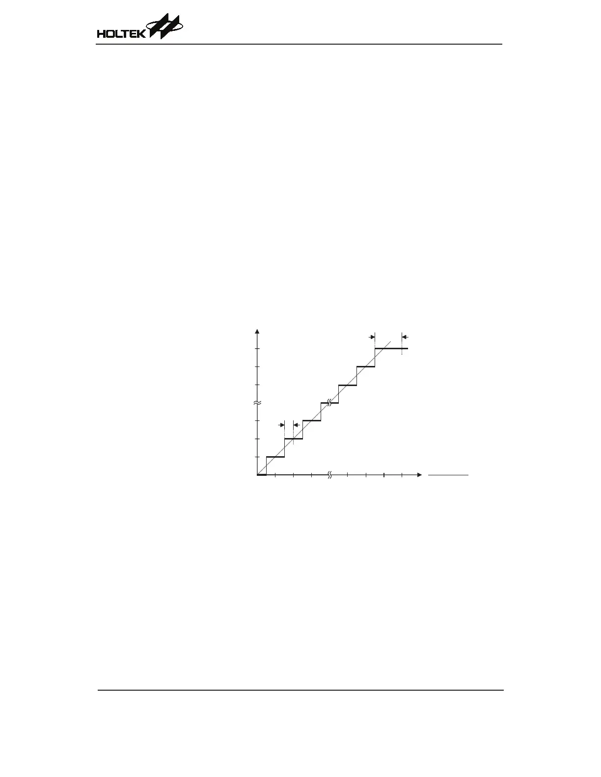
A/D Transfer Function
Asthedevicescontaina12-bitA/Dconverter,itsfull-scaleconverteddigitisedvalueisequalto
FFFH.Sincethefull-scaleanaloginputvalueisequaltotheV
DD
orV
REF
voltage,thisgivesasingle
bitanaloginputvalueofV
DD
orV
REF
dividedby4096.
1LSB=(V
DD
orV
REF
)÷4096
TheA/DConverterinputvoltagevaluecanbecalculatedusingthefollowingequation:
A/Dinputvoltage=A/Doutputdigitalvalue×(V
DD
orV
REF
)÷4096
Thediagramshowstheidealtransferfunctionbetweentheanaloginputvalueandthedigitised
outputvaluefortheA/Dconverter.Exceptforthedigitisedzerovalue,thesubsequentdigitised
valueswillchangeatapoint0.5LSBbelowwheretheywouldchangewithouttheoffset,andthe
lastfullscaledigitisedvaluewillchangeatapoint1.5LSBbelowtheV
DD
orV
REF
level.
Ideal A/D Transfer Function