Rev. 2.50 240 June 22, 2017 Rev. 2.50 241 June 22, 2017
HT66F20/HT66F30/HT66F40/HT66F50/HT66F60
HT66FU30/HT66FU40/HT66FU50/HT66FU60
A/D Flash MCU with EEPROM
HT66F20/HT66F30/HT66F40/HT66F50/HT66F60
HT66FU30/HT66FU40/HT66FU50/HT66FU60
A/D Flash MCU with EEPROM
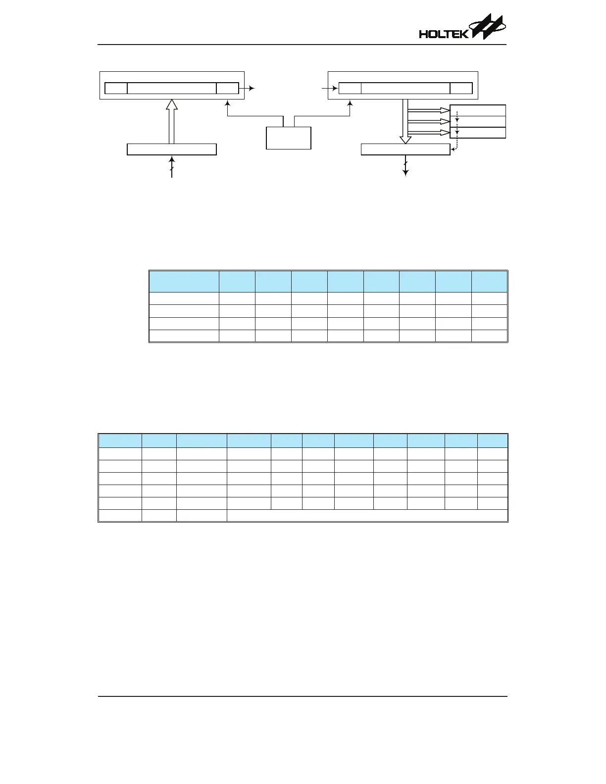
UART Data Transfer Scheme
MSB LSB
…………………………
Transmitter Shift Register (TSR)
MSB LSB
…………………………
Receiver Shift Register (RSR)
TX Pin RX Pin
Baud Rate
Generator
TX Register (TXR) RX Register (RXR)
Buffer 1
Buffer 2
Buffer 3
Data to be transmitted Data received
UART Data Transfer Scheme
UART Commands
TherearebothreadandwritecommandsfortheUARTModule.Forreadingandwritingtoregisters
bothcommandandaddressinformationiscontainedwithinasinglebyte.Theformatforreadingand
writingisshowninthefollowingtable.
Command Type Bit 7 Bit 6 Bit 5 Bit 4 Bit 3 Bit 2 Bit 1 Bit 0
Read FIFO 0 0 0 0 0 × × ×
Read Register 0 0 0
1 0 A2 A1 A0
Write FIFO 0 0 0 0
1 × × ×
Write Register 0 0 0
1 1 A2 A1 A0
Note: "×" here stands for don't care
UART Status and Control Registers
TherearesixregistersassociatedwiththeUARTfunction.TheUSR,UCR1,UCR2andUCR3
registerscontroltheoverallfunctionoftheUARTmodule,whiletheBRGregistercontrolstheBaud
rate.Theactualdatatobetransmittedandreceivedontheserialinterfaceismanagedthroughthe
TXR/RXRdataregister.
A[2:0] Name Reset Bit 7 Bit 6 Bit 5 Bit 4 Bit 3 Bit 2 Bit 1 Bit 0
00H USR
0000 1011 PERR NF FERR OERR RIDLE RXIF TIDLE TXIF
01H UCR1 0000 0×00 UARTEN BNO PREN PRT STOPS TXBRK RX8 TX8
02H UCR2 0000 0000 TXEN RXEN BRGH ADDEN WAKE RIE TIIE TEIE
03H BRG ×××× ××××
BRG7 BRG6 BRG5 BRG4 BRG3 BRG2 BRG1 BRG0
04H UCR3 0--- ---- URST — — — — — — —
05H~07H Unused ---- ---- Reserved
UART Register Summary