Rev. 2.50 174 June 22, 2017 Rev. 2.50 175 June 22, 2017
HT66F20/HT66F30/HT66F40/HT66F50/HT66F60
HT66FU30/HT66FU40/HT66FU50/HT66FU60
A/D Flash MCU with EEPROM
HT66F20/HT66F30/HT66F40/HT66F50/HT66F60
HT66FU30/HT66FU40/HT66FU50/HT66FU60
A/D Flash MCU with EEPROM
A/D Operation
TheSTARTbitintheADCR0registerisusedtostartandresettheA/Dconverter.Whenthe
microcontrollersetsthisbitfromlowtohighandthenlowagain,ananalogtodigitalconversion
cyclewillbeinitiated.WhentheSTARTbitisbroughtfromlowtohighbutnotlowagain,theEOCB
bitintheADCR0registerwillbesethighandtheanalogtodigitalconverterwillbereset.Itisthe
STARTbitthatisusedtocontroltheoverallstartoperationoftheinternalanalogtodigitalconverter.
TheEOCBbitintheADCR0registerisusedtoindicatewhentheanalogtodigitalconversion
processiscomplete.Thisbitwillbeautomaticallysetto0bythemicrocontrollerafteraconversion
cyclehasended.Inaddition,thecorrespondingA/Dinterruptrequestagwillbesetintheinterrupt
controlregister,andiftheinterruptsareenabled,anappropriateinternalinterruptsignalwillbe
generated.ThisA/DinternalinterruptsignalwilldirecttheprogramflowtotheassociatedA/D
internalinterruptaddressforprocessing.IftheA/Dinternalinterruptisdisabled,themicrocontroller
canbeusedtopolltheEOCBbitintheADCR0registertocheckwhetherithasbeenclearedasan
alternativemethodofdetectingtheendofanA/Dconversioncycle.
TheclocksourcefortheA/Dconverter,whichoriginatesfromthesystemclockf
SYS
,canbechosen
tobeeitherf
SYS
orasubdividedversionoff
SYS
.Thedivisionratiovalueisdeterminedbythe
ADCK2~ADCK0bitsintheADCR1register.
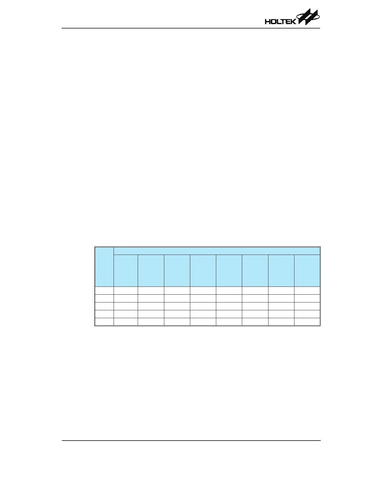
AlthoughtheA/Dclocksourceisdeterminedbythesystemclockf
SYS
,andbybitsADCK2~ADCK0,
therearesomelimitationsonthemaximumA/Dclocksourcespeedthatcanbeselected.Asthe
minimumvalueofpermissibleA/Dclockperiod,t
ADCK
,is0.5μs,caremustbetakenforsystemclock
frequenciesequaltoorgreaterthan4MHz.Forexample,ifthesystemclockoperatesatafrequency
of4MHz,theADCK2~ADCK0bitsshouldnotbesetto000.DoingsowillgiveA/Dclockperiods
thatarelessthantheminimumA/DclockperiodwhichmayresultininaccurateA/Dconversion
values.Refertothefollowingtableforexamples,wherevaluesmarkedwithanasterisk*show
where,dependinguponthedevice,specialcaremustbetaken,asthevaluesmaybelessthanthe
speciedminimumA/DClockPeriod.
f
SYS
A/D Clock Period (t
ADCK
)
ADCK2,
ADCK1,
ADCK0
=000
(f
SYS
)
ADCK2,
ADCK1,
ADCK0
=001
(f
SYS
/2)
ADCK2,
ADCK1,
ADCK0
=010
(f
SYS
/4)
ADCK2,
ADCK1,
ADCK0
=011
(f
SYS
/8)
ADCK2,
ADCK1,
ADCK0
=100
(f
SYS
/16)
ADCK2,
ADCK1,
ADCK0
=101
(f
SYS
/32)
ADCK2,
ADCK1,
ADCK0
=110
(f
SYS
/64)
ADCK2,
ADCK1,
ADCK0
=111
1MHz 1μs 2μs 4μs 8μs 16μs 32μs 64μs Undened
2MHz 500ns 1μs 2μs 4μs 8μs 16μs 32μs Undened
4MHz 250ns* 500ns 1μs 2μs 4μs 8μs 16μs Undened
8MHz
125ns* 250ns* 500ns 1μs 2μs 4μs 8μs Undened
12MHz 83ns* 167ns* 333ns* 667ns 1.33μs 2.67μs 5.33μs Undened
A/D Clock Period Examples
Controllingthepoweron/offfunctionoftheA/Dconvertercircuitryisimplementedusingthe
ADOFFbitintheADCR0register.ThisbitmustbezerotopowerontheA/Dconverter.When
theADOFFbitisclearedtozerotopowerontheA/Dconverterinternalcircuitryacertaindelay,
asindicatedinthetimingdiagram,mustbeallowedbeforeanA/Dconversionisinitiated.Even
ifnopinsareselectedforuseasA/DinputsbyclearingtheACE11~ACE0bitsintheACERH
andACERLregisters,iftheADOFFbitiszerothensomepowerwillstillbeconsumed.Inpower
consciousapplicationsitisthereforerecommendedthattheADOFFissethightoreducepower
consumptionwhentheA/Dconverterfunctionisnotbeingused.
ThereferencevoltagesupplytotheA/DConvertercanbesuppliedfromeitherthepositivepower
supplypin,VDD,orfromanexternalreferencesourcessuppliedonpinVREF.Thedesiredselection
ismadeusingtheVREFSbit.AstheVREFpinispin-sharedwithotherfunctions,whentheVREFS
bitissethigh,theVREFpinfunctionwillbeselectedandtheotherpinfunctionswillbedisabled
automatically.