Rev. 2.50 170 June 22, 2017 Rev. 2.50 171 June 22, 2017
HT66F20/HT66F30/HT66F40/HT66F50/HT66F60
HT66FU30/HT66FU40/HT66FU50/HT66FU60
A/D Flash MCU with EEPROM
HT66F20/HT66F30/HT66F40/HT66F50/HT66F60
HT66FU30/HT66FU40/HT66FU50/HT66FU60
A/D Flash MCU with EEPROM
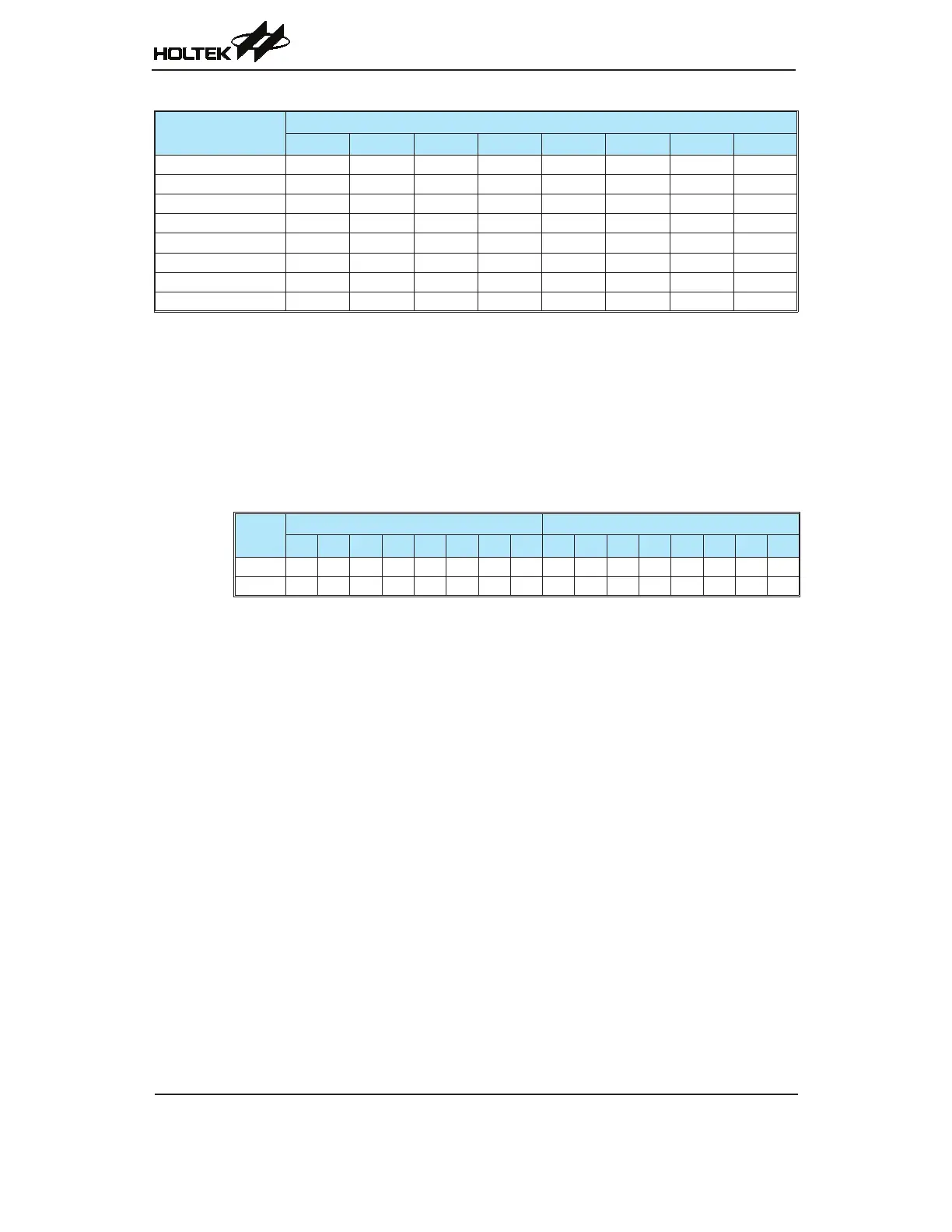
Register Name
Bit
7 6 5 4 3 2 1 0
ADRL(ADRFS=0) D3 D2
D1 D0 — — — —
ADRL(ADRFS=1) D7 D6 D5 D4 D3 D2 D1 D0
ADRH(ADRFS=0)
D11 D10 D9 D8 D7 D6 D5 D4
ADRH(ADRFS=1) — — — — D11 D10 D9 D8
ADCR0 START EOCB ADOFF ADRFS ACS3 ACS2
ACS1 ACS0
ADCR1 ACS4 V125EN — VREFS — ADCK2 ADCK1 ADCK0
ACERL
ACE7 ACE6 ACE5 ACE4 ACE3 ACE2 ACE1 ACE0
ACERH — — — —
ACE11 ACE10 ACE9 ACE8
HT66F60 A/D Converter Register List
A/D Converter Data Registers – ADRL, ADRH
Asthedevicescontainaninternal12-bitA/Dconverter,theyrequiretwodataregisterstostorethe
convertedvalue.Theseareahighbyteregister,knownasADRH,andalowbyteregister,known
asADRL.Aftertheconversionprocesstakesplace,theseregisterscanbedirectlyreadbythe
microcontrollertoobtainthedigitisedconversionvalue.Asonly12bitsofthe16-bitregisterspace
isutilised,theformatinwhichthedataisstorediscontrolledbytheADRFSbitintheADCR0
registerasshownintheaccompanyingtable.D0~D11aretheA/Dconversionresultdatabits.Any
unusedbitswillbereadaszero.
ADRFS
ADRH ADRL
7 6 5 4 3 2 1 0 7 6 5 4 3 2 1 0
0
D11 D10 D9 D8 D7 D6 D5 D4 D3 D2 D1 D0 0 0 0 0
1 0 0 0 0 D11 D10 D9 D8 D7 D6 D5 D4 D3 D2 D1 D0
A/D Data Registers
A/D Converter Control Registers – ADCR0, ADCR1, ACERL, ACERH
TocontrolthefunctionandoperationoftheA/Dconverter,threeorfourcontrolregistersknownas
ADCR0,ADCR1,ACERLandACERHareprovided.These8-bitregistersdenefunctionssuch
astheselectionofwhichanalogchannelisconnectedtotheinternalA/Dconverter,thedigitised
dataformat,theA/DclocksourceaswellascontrollingthestartfunctionandmonitoringtheA/D
converterendofconversionstatus.TheACS3~ACS0bitsintheADCR0registerandACS4bitis
theADCR1registerdenetheADCinputchannelnumber.Asthedevicecontainsonlyoneactual
analogtodigitalconverterhardwarecircuit,eachoftheindividual8or12analoginputsmustbe
routedtotheconverter.ItisthefunctionoftheACS4~ACS0bitstodeterminewhichanalogchannel
inputpinsorinternal1.25VisactuallyconnectedtotheinternalA/Dconverter.
TheACERHandACERLcontrolregisterscontaintheACER11~ACER0bitswhichdetermine
whichpinsonPortA,PE6,PE7,PF0andPF1areusedasanaloginputsfortheA/Dconverterinput
andwhichpinsarenottobeusedastheA/Dconverterinput.Settingthecorrespondingbithighwill
selecttheA/Dinputfunction,clearingthebittozerowillselecteithertheI/Oorotherpin-shared
function.WhenthepinisselectedtobeanA/Dinput,itsoriginalfunctionwhetheritisanI/Oor
otherpin-sharedfunctionwillberemoved.Inaddition,anyinternalpull-highresistorsconnectedto
thesepinswillbeautomaticallyremovedifthepinisselectedtobeanA/Dinput.