Rev. 2.50 20 June 22, 2017 Rev. 2.50 21 June 22, 2017
HT66F20/HT66F30/HT66F40/HT66F50/HT66F60
HT66FU30/HT66FU40/HT66FU50/HT66FU60
A/D Flash MCU with EEPROM
HT66F20/HT66F30/HT66F40/HT66F50/HT66F60
HT66FU30/HT66FU40/HT66FU50/HT66FU60
A/D Flash MCU with EEPROM
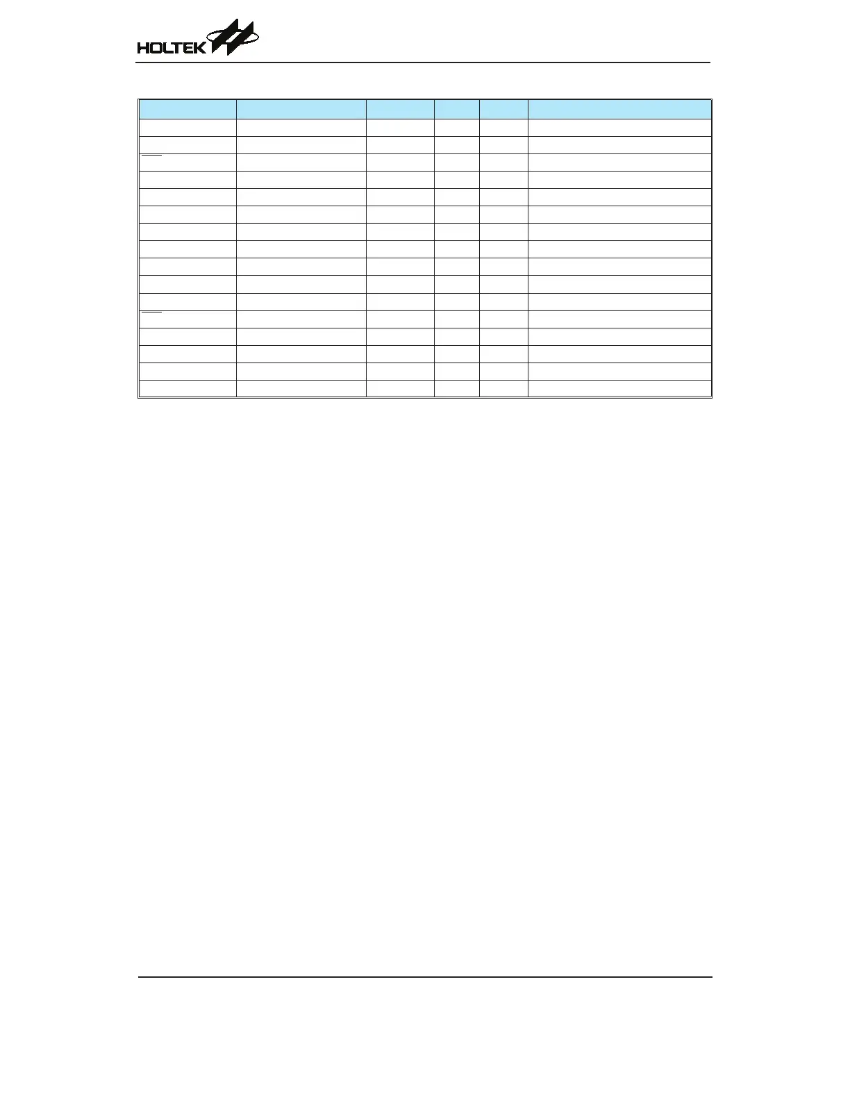
Pin Name Function OP I/T O/T Pin-Shared Mapping
SDI
SPI Data input PRM0 ST — PA6 or PD2 or PB7
SDO SPI Data output PRM0 — CMOS PA5 or PD3 or PB6
SCS SPI Slave Select PRM0 ST CMOS PB5 or PD0 or PD7
SCK SPI Serial Clock PRM0 ST CMOS PA7 or PD1 or PD6
SCL I
2
C Clock PRM0 ST NMOS PA7 or PD1 or PD6
SDA I
2
C Data PRM0 ST NMOS PA6 or PD2 or PB7
SCOM0~SCOM3 SCOM0~SCOM3 SCOMC — SCOM PC0, PC1, PC6, PC7
OSC1 HXT/ERC pin CO HXT — PB1
OSC2 HXT pin CO — HXT PB2
XT1 LXT pin CO LXT — PB3
XT2 LXT pin CO — LXT PB4
RES Reset input CO ST — PB0
VDD
Power supply* — PWR — —
AVDD
ADC power supply* — PWR — —
VSS
Ground** — PWR — —
AVSS
ADC ground** — PWR — —
Note:I/T:Inputtype; O/T:Outputtype
OP:Optionalbycongurationoption(CO)orregisteroption
PWR:Power; CO:Congurationoption; ST:SchmittTriggerinput
CMOS:CMOSoutput; NMOS:NMOSoutput
SCOM:SoftwarecontrolledLCDCOM; AN:Analogsignal
HXT:Highfrequencycrystaloscillator
LXT:Lowfrequencycrystaloscillator
*:VDDisthedevicepowersupplywhileAVDDistheADCpowersupply.TheAVDDpinisbonded
togetherinternallywithVDD.
**:VSSisthedevicegroundpinwhileAVSSistheADCgroundpin.TheAVSSpinisbondedtogether
internallywithVSS.
AsthePinDescriptionSummarytableappliestothepackagetypewiththemostpins,notalloftheabove
listedpinsmaybepresentonpackagetypeswithsmallernumbersofpins.