Rev. 2.50 236 June 22, 2017 Rev. 2.50 237 June 22, 2017
HT66F20/HT66F30/HT66F40/HT66F50/HT66F60
HT66FU30/HT66FU40/HT66FU50/HT66FU60
A/D Flash MCU with EEPROM
HT66F20/HT66F30/HT66F40/HT66F50/HT66F60
HT66FU30/HT66FU40/HT66FU50/HT66FU60
A/D Flash MCU with EEPROM
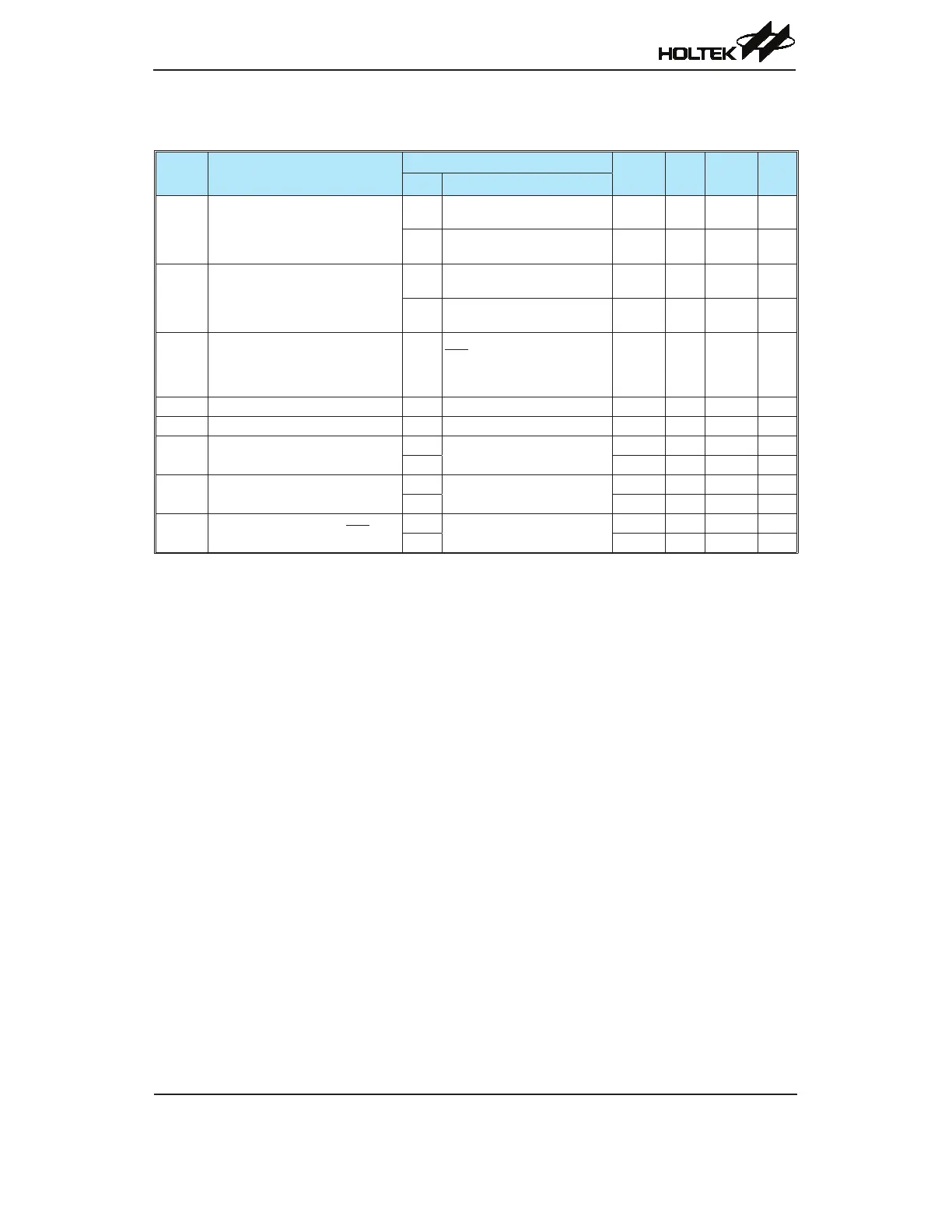
UART Module D.C. Characteristics
Ta=25°C
Symbol Parameter
Test Conditions
Min. Typ. Max. Unit
V
DD
Conditions
I
DD1
Operating Current *
(SPI Enabled, UART disabled)
3.0V
f
CLKI
=12MHz, SCK=f
CLKI
/4,
Output no load
— — 1.0 mA
5.0V
f
CLKI
=16MHz, SCK=f
CLKI
/4,
Output no load
— — 2.0 mA
I
DD2
Operating Current *
(SPI enabled, UART enabled)
2.2V
f
CLKI
=6MHz, SCK=f
CLKI
/4,
Output no load
— — 4.2 mA
5.0V
f
CLKI
=12MHz, SCK=f
CLKI
/4,
Output no load
— — 4.8 mA
I
STB
Standby Current *
(SPI disabled, UART disabled)
5.0V
f
CLKI
=16MHz, SCK=f
CLKI
/4,
SCS=V
DD
, UARTEN=0,
TXEN=1, RXEN=1, SDI=H,
RX=H, Output no load
— — 0.6 μA
V
IL
Input Low Voltage for RX Ports — — 0 — 0.3V
DD
V
V
IH
Input High Voltage for RX Ports — — 0.7V
DD
— V
DD
V
I
OL
TX Port Sink Current
3.0V
V
O
=0.1V
DD
2.5 5.0 — mA
5.0V
10.0 25.0 — mA
I
OH
RX Port Source Current
3.0V
V
O
=0.9V
DD
-1.5 -3.0 — mA
5.0V -5.0 -8.0 — mA
R
PH
Pull-high Resistance for SCS only
3.0V
—
20 60
100 kΩ
5.0V
10 30 50 kΩ
Note:"*"TheoperatingcurrentI
DD1
listedhereistheadditionalcurrentconsumedwhentheslaveSPIinterface
intheUARTmoduleisenabledandtheUARTinterfaceisdisabled.Similarly,theoperatingcurrent
I
DD2
hereistheadditionalcurrentconsumedwhenboththeslaveSPIinterfaceandUARTinterfaceare
enabled.IftheUARTmoduleisenabled,eitherI
DD1
orI
DD2
shouldbeaddedtocalculatetherelevant
operatingcurrentofthedevicefordifferentconditions.Tocalculatethestandbycurrentforthewhole
device,thestandbycurrentshownaboveshouldbetakenintoaccount.