Do you have a question about the Huawei MS2131 and is the answer not in the manual?
Details the MS2131's wireless network access capabilities and supported modes.
Provides a summary of the MS2131's features and technical specifications.
Illustrates the functional block diagram of the MS2131, showing key modules.
Shows the application diagram of the MS2131's ports, including USB, SIM, and antenna.
Introduces the MS2131's interfaces, focusing on USB and power ports.
Details the USB port, its protocol support, and essential reference circuits for host design.
Explains the MS2131's power port requirements and considerations for host power supply design.
Describes the SIM card port, its voltage support, and lack of external design needs.
Lists the supported working frequency bands for the MS2131 across different technologies.
Details Total Isotropic Sensitivity (TIS) and Total Radiated Power (TRP) specifications.
Explains Total Isotropic Sensitivity (TIS) and provides its specifications for the MS2131.
Defines Total Radiated Power (TRP) and lists its optimal specifications for the MS2131.
Provides critical layout requirements for host PCBs to ensure optimal MS2131 antenna performance.
Describes the microwave testing chamber and test items for antenna performance.
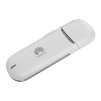
Specifies the physical dimensions and weight of the MS2131 device.
Details design requirements for the host structure when integrating the MS2131.
Provides the outline dimensions and PCB thickness requirements for the USB connector.
Outlines rules for peripheral placement and routing to maintain MS2131 wireless performance.
Details the power supply voltage range and source for the MS2131 via USB.
Explains power consumption and transient behavior of the MS2131 in 2G (GSM) mode.
Describes power characteristics and transmission in 3G networks, noting no time correlation.
Lists power consumption specs for 3G networks, including standby and data modes.
Outlines requirements for peripheral power design to handle voltage drops during GSM transmission.
Recommends a power structure with DC-DC output, switching diode, and current limiting for control.
Advises 85% derating for external power supply voltage and current for converters/LDOs.
Provides specific rules for peripheral power cable routing, capacitors, and diodes.
Covers rules for signal integrity, conductivity, and USB differential signal routing.
Discusses power design's impact on EMC, spectrum, and sensitivity, with quality rules.
Details rules for power cable width and USB signal impedance and routing.
Specifies cable width and copper thickness for power routing to handle peak currents.
Explains 90 Ω impedance requirements for USB signal cables and grounding.
Covers grounding for USB signals and ensuring reference ground continuity.
Recommends PCB layers, capacitors, TVS for ESD protection, and signal cable routing.
Suggests shell design for ESD protection, particularly for SIM card and connector areas.
Specifies the operating voltage limitation for the MS2131 to prevent permanent damage.
Details the operating temperature and humidity ranges for the MS2131.
Covers input power specifications and working current details for the MS2131.
Lists specifications for the MS2131's input power, including voltage and ripple.
Refers to appendix for MS2131 working current data in various scenarios with typical power.
Presents MS2131 reliability test conditions and results, including drop and vibration tests.
Provides working current data for MS2131 in common scenarios across different bands.
Presents Over-the-Air (OTA) test data, specifically Total Isotropic Sensitivity (TIS).
Refers to a thermal test report for the MS2131.
| Category | Modem |
|---|---|
| Maximum Download Speed | 150 Mbps |
| Maximum Upload Speed | 50 Mbps |
| Interface | USB 2.0 |
| Cellular technology | 4G LTE |
| Weight | 30 g |
| SIM Type | Standard SIM |
| Download speed | 150 Mbps |
| Upload speed | 50 Mbps |