8.3 Cable Routing Rules
8.3.1 Power Design
The power consumption of the MS2131 varies by network standard. Working in GSM mode,
the MS2131 has a peak current of larger than 2 A. To ensure a sufficient power capacity and
minimize the voltage drop caused by cable routing, a 100-mil cable routing width is
recommended and the finish copper thickness is 1 OZ. If possible, maximize the power cable
routing width.
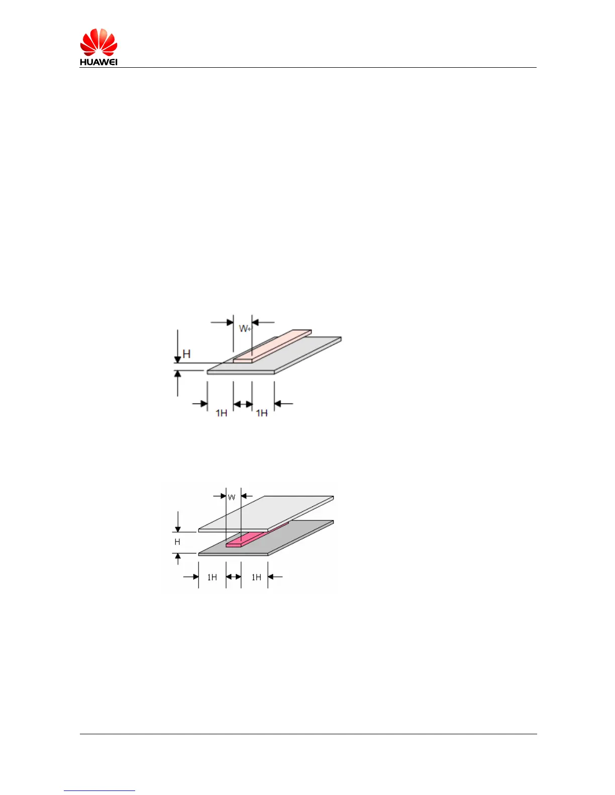
8.3.2 USB Signal Cable Routing Design
The impedance for the USB signal cable on the user PCB must be 90 Ω. The impedance is
dependent on the dielectric constant, cable width, and the distance from the ground. Figure
8-1 and Figure 8-2 show the structures and stacking designs of the 90 Ω impedance
microstrips and strip lines that can be adopted for the cabling impedance design.
Figure 8-1 Microstrip structure
Figure 8-2 Strip line structure
You can use either of the preceding ways to design the 90 Ω cabling impedance.
Note that the USB signal cabling impedance must be dedicatedly designed and the two sides
of the USB must be fully surrounded by grounds.