‐
5.1.3 Audio Module
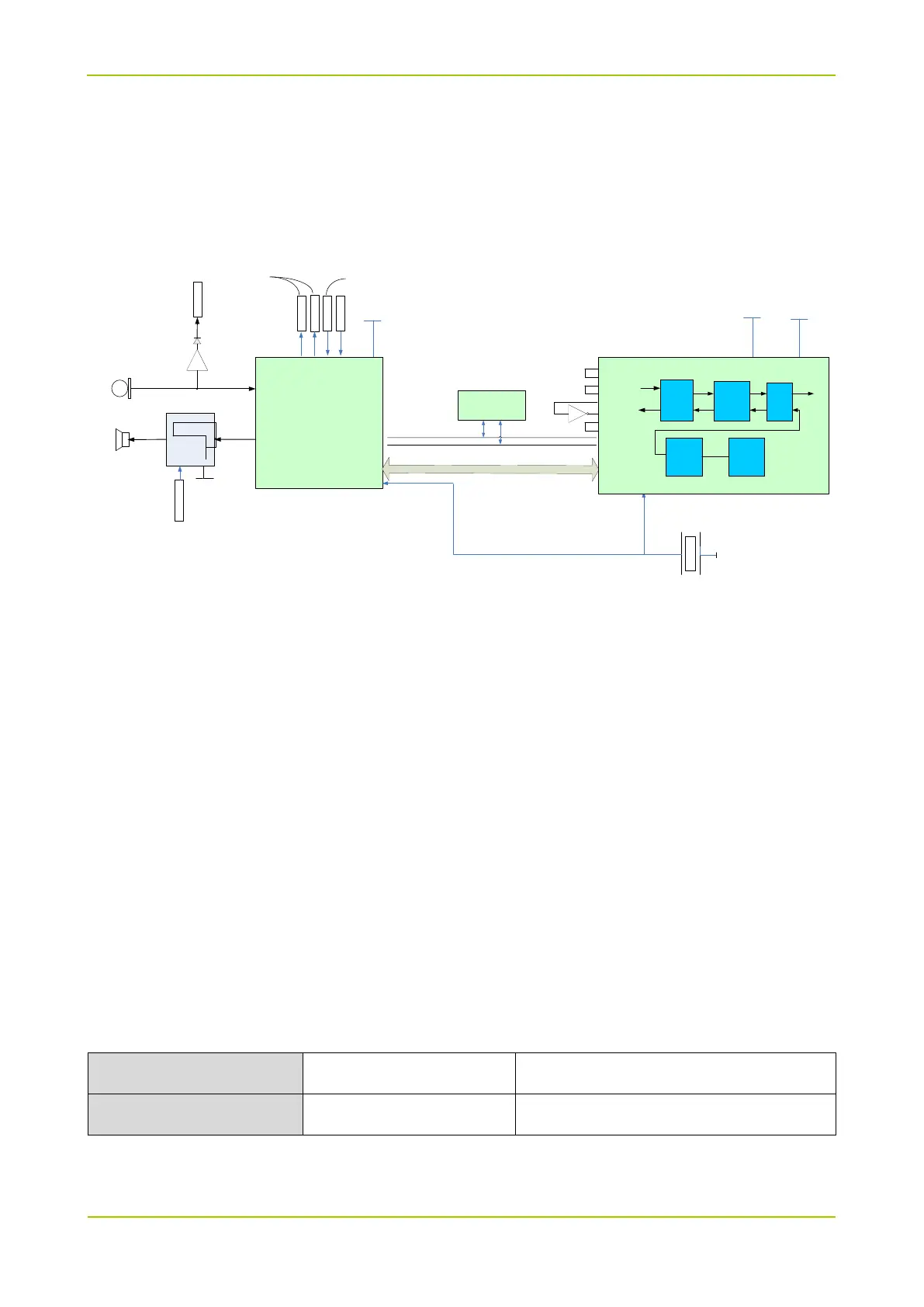
Audio Diagram
The audio processing section uses SCT3928 and TLV320AIC3204. The audio amplifier uses TDA2822D.
The diagram is as follows:
CODEC
TLV320AIC3204
AMP
TDA2822D
MCLK
BCLK
WCLK
DIN
DOUT
MCLK
VDD3V3
12.288MHZ
SCL
SDA
Security Key
I2S
VOICE
CODER
Protoccol
Stack
4FSK
FM
Demod
Channel
Selection
SCT3928
S0CLK
S0FS
S0DO
S0DI
S1CLK
S1FS
S1DO
S1DI
CLKIN
SCL
SDA
FLASH_CLK
FLASH_CE
FLASH_DI
FLASH_DO
MOD_VCO
MOD_REF
AFDET
BEEP
3V0A
BAT
3V0D
1V2
LOR
LOL/R
IN3R
IN1L
HPL/R
IN2L
AF_MUTE
VOX
These two signals go to FGU for
modulation
This signal is down converted by
RX end and output by BA4116
RX path
The signal demodulated by RF module is sent to the input port of the third path of TLV320AIC3204
for internal amplifying. After AD conversion, the signal is sent to SCT3928 via I2S interface for
internal processing. Then the signal is sent to TLV320AIC3204 via I2S interface for DA conversion
and internal amplifying. Finally, the audio signal is output from the HPL/R port of TLV320AIC3204 to
audio power amplifier TDA2822D for amplifying, so as to drive the speaker.
TX path
The audio signal received by the MIC is divided into two paths: one path is processed and sent to
MCU for VOX sampling; the other path is sent to TLV320AIC3204 for AGC amplifying. After AD
conversion, the latter path of signal is sent to SCT3928 via I2S interface for internal processing. Then
it is sent to TLV320AIC3204 via I2S interface for DA conversion and amplifying. Finally, the audio
signal is output to FGU for two-path modulation via the LOL/R port of TLV320AIC3204.
Audio Power Amplifier
Main parameters of TDA2822 are listed in the table below:
Rated Power (P
o
)
0.5 W R L =16 Ω
Maximum Power (P
max
)
1.6 W R L =16 Ω