‐
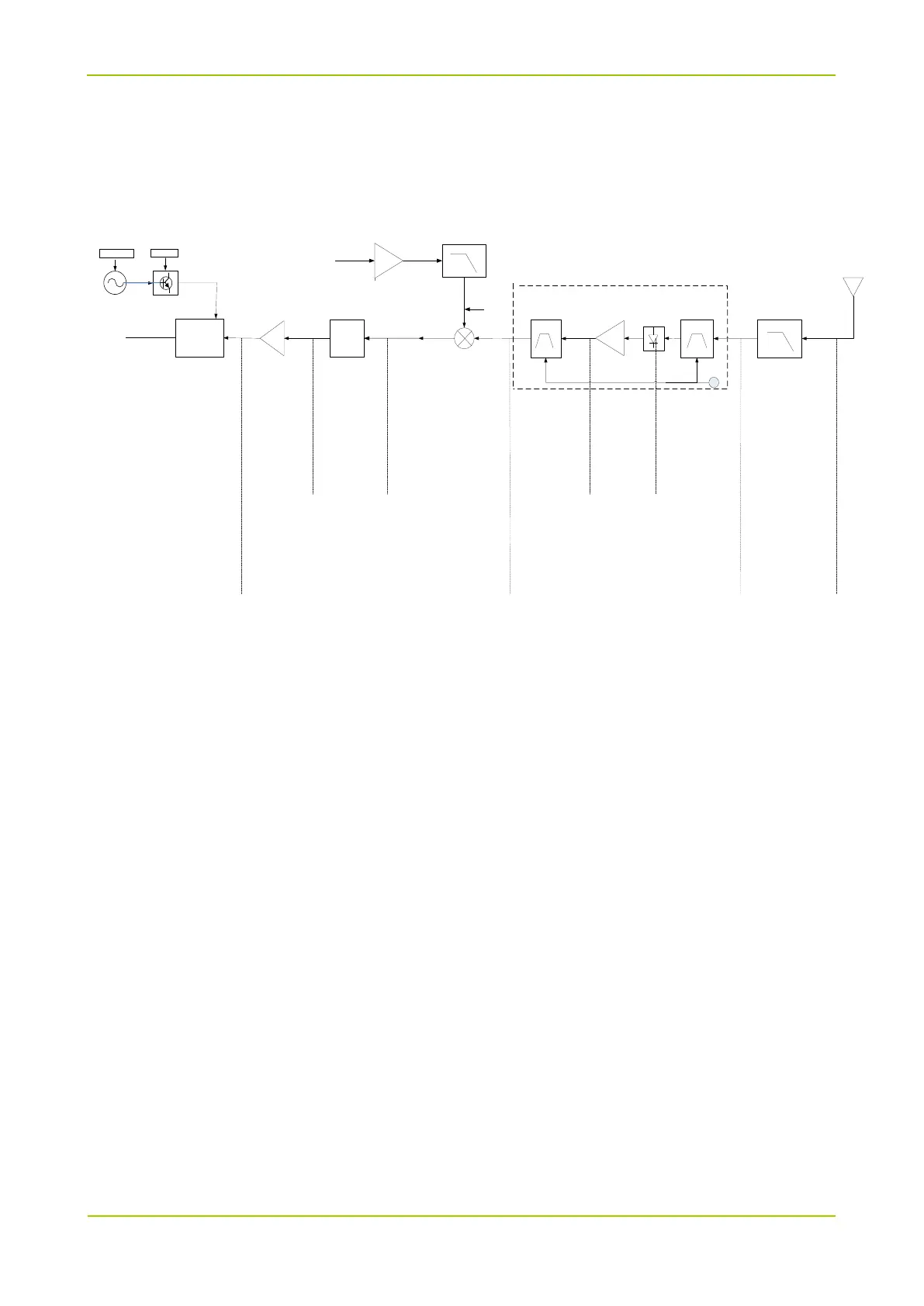
5.2.2 Receiver Circuit
The receiver circuit is mainly composed of RF band-pass filter, low-noise amplifier, mixer, IF filter, IF
amplifier and IF processor.
Low-pass Filter
Band-pass Filter1
Low-Noise Amp
AT-41511
Band-pass Filter2
Mixer
HSMS-2827
IF Filter
IF Processor
IF Amp
2SC5108
ANT
LPF
S21≤1.5dB
Ripple Inband≤ 1dB
Stop band attenuation: -30dBc
S21≥ -0.8dB
S11≤ -15dB
S22≤ -15dB
Ripple Inband≤ 0.4dB
Stop band attenuation: -50dBc
TV
Tuning voltage:0.5-2.8V
Linear Gain≥ 12dB
S11≤ -15dB
S22≤ -15dB
S12≤ -30dB
Rejection at -1/2IF≥ 15dB
Rejection at -2IF≥ 80dB
Rejection at 2Fin-3IF≥ 55dB
IIP3 ≥ 1dBm
Distortion ≤ 2%
Insertion Loss≤ 2dB
S11≤ -15dB
S22≤ -15dB
Rejection at -2IF ≥ 40dB
Rejection at -1/2IF > 8dB
Vdd:3V3dc
Gain≥ 18dB
Current Drain≤ 8mA
S11≤ -15dB
S22≤ -15dB
S12≤ -25dB
NF≤1.5dB
Insertion Loss≤ 3dB
S11≤ -15dB
S22≤ -15dB
Rejection at -2IF ≥ 40dB
Rejection at -1/2IF >12dB
Lo
Lo Amp
2SC3356
Vdd:3V3dc
Gain≥ 20dB
Current Drain≤ 3mA
S11≤ -15dB
S22≤ -15dB
S12≤ -25dB
output level≤ -11dBm
Gain≥ 4dB
Distortion ≤3%
Ripple Inband≤ 1dB
3dB Bandwith≥±6KHz
Attenuation:
@±12.5kHz≥18dBc
@±25kHz≥ 40dBc
@±2*2nd IF≥ 85dBc
Vdd:3V3dc
Input level≥ -99dBm
2nd Lo:
Vdd:3Vdc
Frequency:IF
Current Drain≤ 2mA
output level≤ -22dBm
Lo input level≥7dBm
Attenuator Protect
RB706F
3V3dc
Double Circuit
2SC5108
3V3FGU
VCTCXO
19.2MHz
BA4116FV
AF OUT
Centre Frequency:IF
Insertion loss≤ 5dB
3dB Bandwith≥±5KHz
Ripple Inband≤ 1dB
Attenuation:
@±12.5kHz≥18dBc
@±25kHz≥ 40dBc
@±2*2nd IF≥ 85dBc
S11≤ -15dB
S22≤ -15dB
IIP3≥ 18dBm
Conversion loss≥-7dB
IIP3≥ 15dBm
Isolation :
of LO to RF> 30dB
of RF to IF> 25dB
of LO to IF> 30dB
Lo input level≥7dBm
NF≤7
dB
Receiver Front-end
The HF signal from the low-pass filter passes through the electrically tunable first-stage band-pass filter
controlled via APC/TV1 level, then the filter removes out-of-band interference signal and sends desired
band-pass signal to the low-noise amplifier (Q602). The amplified signal goes to the second-stage
band-pass filter which is also controlled via APC/TV1 level, and the filter removes out-of-band
interference signal generated during amplification, and sends the filtered HF signal to the mixer.
The filtered HF signal goes to the mixer (D607) through the RF band-pass filter and low-noise amplifier.
Meanwhile, the first local oscillator (LO) signal generated by VCO also goes to the mixer (D607) through
the low-pass filter. In the mixer, the first LO signal and the HF signal are mixed to generate the first IF
signal. Then the first IF signal passes through the frequency selection circuit (composed of one LC) to
have carriers (except the first IF signal) suppressed, so as to increase the isolation between the mixer
and the IF filter. After that, the first IF signal is filtered by the crystal filter (Z601), and is sent to the IF
amplifier circuit (Q604) for amplification. Then the amplified signal goes to the IF processor (BA4116FV)
for processing.