‐
Contents
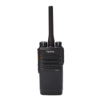
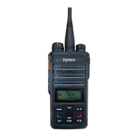
1. Product Controls .................................................................................................................................. 1
2. Disassembly and Assembly ................................................................................................................ 2
3. Exploded View and Packing Guide .................................................................................................... 4
3.1 Exploded View .................................................................................................................................. 4
3.2 Packing Guide .................................................................................................................................. 6
4. Specifications ....................................................................................................................................... 7
5. Circuit Descriptions ............................................................................................................................. 9
5.1 Baseband Section............................................................................................................................. 9
5.1.1 Power Supply Module ............................................................................................................ 9
5.1.2 Control Module ..................................................................................................................... 10
5.1.3 Audio Module ......................................................................................................................... 11
5.2 RF Section ...................................................................................................................................... 12
5.2.1 Transmitter Circuit ................................................................................................................ 12
5.2.2 Receiver Circuit .................................................................................................................... 14
5.2.3 Frequency Generation Unit (FGU) ....................................................................................... 15
6. Troubleshooting Flow Chart ............................................................................................................. 17
6.1 Control Circuit ................................................................................................................................. 17
6.2 Receiver Circuit .............................................................................................................................. 18
6.3 Transmitter Circuit .......................................................................................................................... 20
6.4 FGU Circuit ..................................................................................................................................... 22
7. Interface Definition ............................................................................................................................. 24
8. Tuning Description ............................................................................................................................. 25
8.1 Required Test Instruments ............................................................................................................. 25
8.2 Tuning Procedures ......................................................................................................................... 25
8.2.1 Tuning the Radio .................................................................................................................. 25
8.2.2 Testing the Radio .................................................................................................................. 28
9. PCB View ............................................................................................................................................. 30
10. Block Diagram .................................................................................................................................. 32
10.1 Overall Diagram of Radio ............................................................................................................. 32
10.2 Block Diagram of Power Supply Circuit ....................................................................................... 33
10.3 B
lock Diagram of Baseband Circuit .............................................................................................. 34
10.4 Block Diagram of Transmitter Circuit ............................................................................................ 35
10.5 Block Diagram of Receiver Circuit ................................................................................................ 36
10.6 Block Diagram of FGU Circuit ...................................................................................................... 37
11. Schematic Diagram .......................................................................................................................... 38
12. Parts List ........................................................................................................................................... 48