Nominal Voltages
The following
regulators
and
their
nominal outputs
can
be
marginally
checked:
Regulator
Nominal Output
+6
TC
1
+6
VAR
12
-12
ROS
3
+6
Ml
4
+6
M2
14 +56 XYl
15
+60
Zl
16
+56
XY2
17
~60
Z2
Marginal Voltage
Limits
The
system
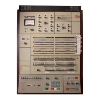
control
panel
meter
is
color
banded
to
show
the
marginal
voltage
limits.
The actual
mar-
ginal voltage
limits
are
dependent on the
results
obtained by running
shmoo-curves.
The following
are
the specified operating
limits.
Regulator
1 (+6 TC)
1
(+6
VAR)
12 (-12 ROS)
3 (+6
Ml)
l
4 (+6
M2)
f
14
(+56
XYl)}
15 (+60
Zl)
16 (+56 XY2)
17 (+60 Z2)
Voltage
Limits
for
Testing
±5%
of
the
optimum
local
storage
setting
±5%
of
the
optimum
local
storage
setting
±2
volts
of
the
optimum
ROS
setting
:t:.S
volt
±4
1/2%
of
the
optimum
main
storage
setting
~
Storage
drivers
may
be
damaged
if
these
voltages
exceed
+68
volts.
Marginal Checking
Procedure
All
marginal
checking
controls
and
indicators
are
mounted on the
system
control
panel. Each control
has
an
indicator
which
is
activated whenever the
margin
control
is
adjusted
from
its
nominal level.
Each
control
varies
the
output of one
regulator.
The independent control of each
regulator
allows
several
inputs to the
same
circuit
to change
at
any
one
time.
The
marginal
voltage
select
switch
de-
termines
which voltage
is
monitored by the
meter.
ERROR CHECKING
Identification
All units of the Model
50
are
identified, grouped,
and provided with a
hardware-checking
scheme
that
detects
errors
at
the unit, indicates them
at
the
system
control
panel, and identifies them
as
to
unit
76
(3/71) Model 50
FEMM
(for instance, power and overload sensing, cooling,
data
flow,
address
checking, channel
errors,
etc.).
1/0
errors
occurring
in a device
or
a
control
unit
are
not included except
for
their
effects on the
channels. Each
CPU'
failure
detection device has a
unique indication in the
error
register.
Failure
Detection
Facilities
The data flow of the CPU
is
checked in eight-bit
bytes.
Control information
is
checked in bytes of
varying
length.
Power
and Cooling
Failure
Detection
Power
and overload
failures
are
indicated by lights
on the maintenance console. The specific unit
at
fault
is
indicated by a tripped
circuit
breaker
or
light in the power distribution unit (PDU).
Thermal
failures
(cooling)
are
indicated on the
maintenance console by lights, one
for
each
frame
(CPU,
storage,
PDU).
CPU
Parity
Checking
The
adder
is
parity
checked and
three
levels
of
failure
detection
are
provided:
half-sum
check,
carry
check, and full-sum
check
(adder output latch
check).
A
half-sum
check indicates
either
incorrect
parity
on data
entering
the
adder
or
a failure in the
adder
half-sum
generation
circuitry.
The
carry
check
indicates a failure in
the
carry
lookahead
cir-
cuitry.
Full-sum
checking, which
is
performed
on
the
adder
output
latches,
checks
that
correct
parity
has
been generated for the developed sum,
or
that
data
entering
the
adder
output
latches
from
an
ex-
ternal
source
(data keys,
address
keys,
selector
channel,
etc.
)
has
correct
parity.
Because
the
adder
is
located in the
data
path
be-
tween any two
registers,
it
is
used
as
the
primary
failure
detection device
for
all
register-to-register
transfers.
The
adder
output latch check
also
pro-
vides the checking
for
all
transfers
to
and
from
main
storage.
The
mover
is
parity
checked
at
both inputs
as
well
as
its
output.
The
three
main groups of
bits
emerging
from
ROS
are
parity
checked. Length
counters
Gland
G2, the
Land
M byte
counters,
and the
MD
counter
are
also
parity
checked. Control
failures
which
are
not
covered
by
error
detection
circuitry,
in general,
cause
data
errors.
For
instance, a
failure
of the
adder
ingates
would
result
in
an
invalid no-bit sum
in the
adder
output
latches.
SAR
ts
also
parity
checked.
 Loading...