iC-TW29 26-BIT ENCODER PROCESSOR
WITH INTERPOLATION AND BiSS INTERFACE
Rev C1, Page 12/28
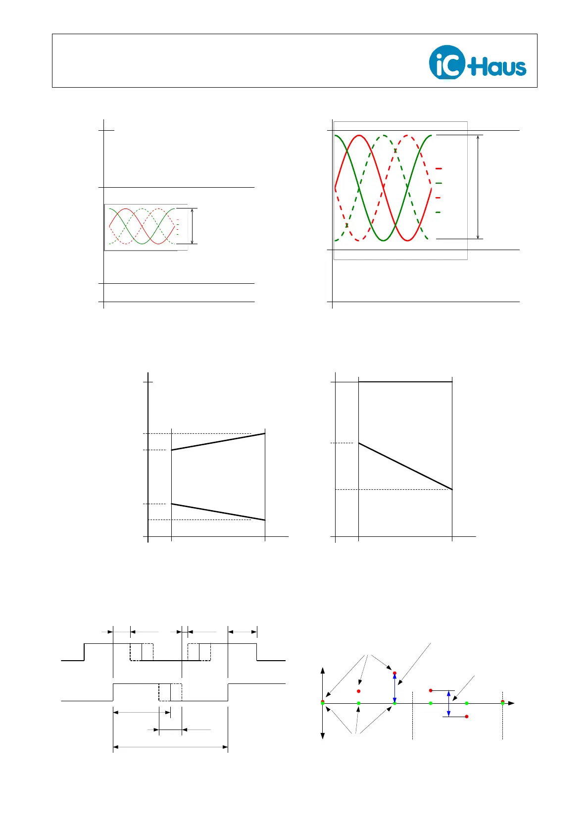
0 V
Maximum Input Voltage
Minimum Input Voltage
Max. Input
Amplitude
(700 mV)
0 V
Maximum Input Voltage
Maximum
Input
Amplitude
(2 V)
Low Input Range
(MAIN_CFG.input = 0 or 1)
High Input Range
(MAIN_CFG.input = 3)
2.2 V
0.35 V
AVDD AVDD
1.0 V
Minimum Input Voltage
Figure 2: Differential Input Amplitude (Ain()diff), Max(SIN+ – SIN–) or Max(COS+ – COS–)
0 V
1.85 V
0.7 V
2.2 V
0.35 V
AVDD
Minimum
Gain
Maximum
Gain
MAIN_CFG.input ≠ 3 or
MAIN_CFG.zero = 0
MAIN_CFG.input = 3 or
MAIN_CFG.zero = 1
0 V
2.0 V
1.0 V
AVDD
Minimum
Gain
Maximum
Gain
Figure 3: Input Common Mode Range, (SIN+ + SIN–)/2, (COS+ + COS–)/2, or (ZERO+ + ZERO–)/2
A
B
t
MTD
t
whi
T (100 %)
AArel
t
AB
ABrel
Figure 4: Description of AB output signals
0° 360°180°
Converter
Error
INL: The maximum absolute error.
DNL: The maximum step
between two consecutive
samples.
Ideal converter
Actual converter
Angular Position
Figure 5:
Denition of integral and differential nonlin-
earity