iC-TW29 26-BIT ENCODER PROCESSOR
WITH INTERPOLATION AND BiSS INTERFACE
Rev C1, Page 14/28
OPERATING REQUIREMENTS: Encoder Link Interface
Operating conditions: AVDD = DVDD = IOVDD = +3.1...+3.6 V, AVSS = DVSS = IOVSS = 0 V, Tj = –40...125 °C
Item Symbol Parameter Conditions Unit
No. Min. Max.
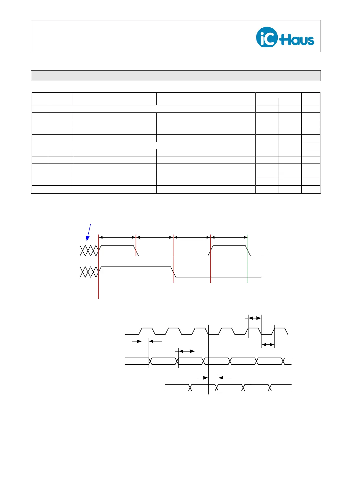
Encoder Link Activation Sequence Timing
I101 T1 Activation Sequence Interval 1 A+ > 2.4 V, A– > 2.4 V 0.25 2 ms
I102 T2 Activation Sequence Interval 2 A+ < 0.8 V, A– > 2.4 V T1 – 10% T1 + 10% ms
I103 T3 Activation Sequence Interval 3 A+ < 0.8 V, A– < 0.8 V T1 – 10% T1 + 10% ms
I104 T4 Activation Sequence Interval 4 A+ > 2.4 V, A– < 0.8 V T1 – 10% T1 + 10% ms
Encoder Link Interface Timing (after activation)
I105 fclk(A+) ELink Clock Frequency Signal driven into A+ 1.0 MHz
I106 t
D1
(A+) ELink Clock Signal Hi Level Duration Signal driven into A+ 200 ns
I107 t
D2
(A+) ELink Clock Signal Lo Level Duration Signal driven into A+ 200 ns
I108 t
S
(A–) ELink Input Setup Time Signal driven into A– 200 ns
I109 t
H
(A–) ELink Input Hold Time Signal driven into A– 200 ns
I110 t
P
(A–) ELink Output Propagation Delay Signal driven out on A– 200 ns
A+
A–
External driver starts to overpower iC-
TW29 by forcing A+ and A– high.
T1
0.25–2 ms
T2
T1 ±10%
T3
T1 ±10%
T4
T1 ±10%
iC-TW29 stops driving A+ and A–.
Encoder Link interface is now active.
Normal operation. iC-TW29 is driving
quadrature signals on A+ and A–.
Figure 7: Encoder Link Activation Sequence
ELCLK (A+)
ELIN (A–)
ELOUT (A–)
T
ELCLK(high)
T
ELCLK(low)
T
ELIN(hold)
T
ELIN(set)
T
ELOUT(prop)
Figure 8: Encoder Link Read and Write Timing