iC-TW29 26-BIT ENCODER PROCESSOR
WITH INTERPOLATION AND BiSS INTERFACE
Rev C1, Page 9/28
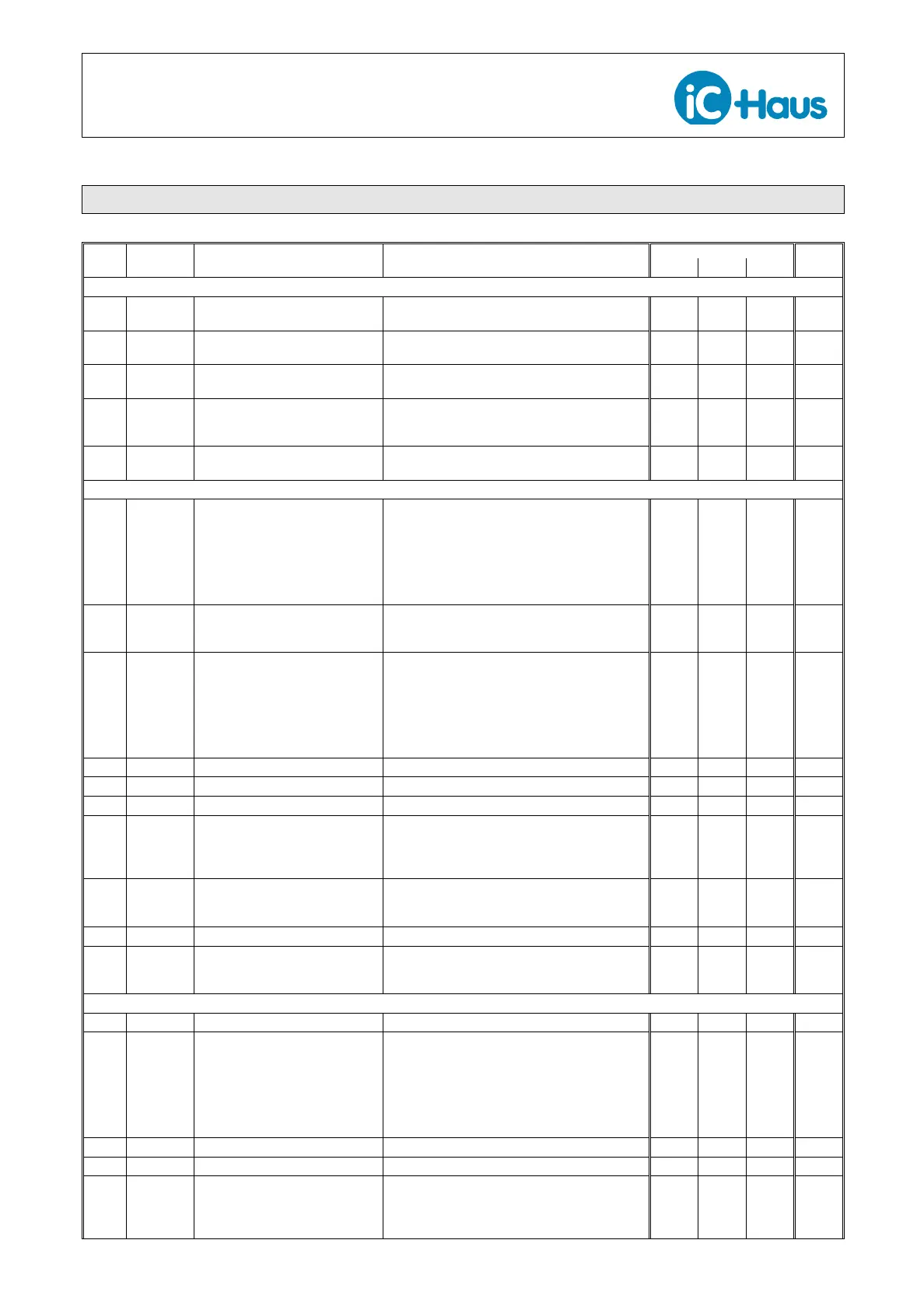
ELECTRICAL CHARACTERISTICS
Operating conditions: AVDD = DVDD = IOVDD = 3.1...3.6 V, Tj = –40...+125 °C, reference point AVSS unless otherwise stated
Item Symbol Parameter Conditions Unit
No. Min. Typ. Max.
Total Device
001 VDD
Permissible Supply Voltage
AVDD, DVDD, IOVDD
3.1 3.6 V
002 I
AVDD
Supply Current into AVDD AVDD, DVDD, IOVDD = 3.3 V, n = 1 kHz,
inter = x256, ABZ and UVW outputs active
15 mA
003 I
DVDD
Supply Current into DVDD AVDD, DVDD, IOVDD = 3.3 V, n = 1 kHz,
inter = x256, ABZ and UVW outputs active
25 mA
004
I
IOVDD
Supply Current into IOVDD
RS422 drivers enabled (MAIN_CFG.rs422 = 1);
quadrature outputs terminated with 120 Ω 85 mA
quadrature outputs open 2 mA
005 I
RST
Reset Current
(I
AVDD
+ I
DVDD
+ I
IAVDD
)
xRST low 1 µA
Signal Inputs and Ampliers: SIN+, SIN–, COS+, COS–
101
Vin() Permissible Input Voltage
Refer to Figure 1
Low Input Range (MAIN_CFG.input = 0 or 1) 0.35 AVDD –
1.1
V
High Input Range (MAIN_CFG.input = 3) 1.0 AVDD V
For High Input Range and MAIN_CFG.input = 2
refer to Figure 1.
102
Ain()diff Permissible Differential Input
Amplitude, Max(SIN+ – SIN–) or
Max(COS+ – COS–)
Refer to Figure 2
Low Input Range (MAIN_CFG.input = 0 or 1) 20 700 mVpp
High Input Range (MAIN_CFG.input = 2 or 3) 65 2000 mVpp
103
Vcm() Permissible Input Common Mode
Range, (SIN+ + SIN–)/2 or
(COS+ + COS–)/2
Refer to Figure 3
Minimum gain (MAIN_CFG.input =/ 3) 0.7 AVDD –
1.45
V
Maximum gain (MAIN_CFG.input =/ 3) 0.35 AVDD –
1.1
V
Minimum gain (MAIN_CFG.input = 3) 2.0 AVDD V
Maximum gain (MAIN_CFG.input = 3) 1.0 AVDD V
104 n() Sin/Cos Input Frequency 700 kHz
105 Vos() Amplier Input Offset Voltage ±15 mV
106 Ilk() Input Leakage Current ±50 nA
108
OFFcorr Correctable Input Offset Voltage
As percentage of input signal amplitude; input
offset voltage is the sum of sensor offset plus
amplier offset (item 105);
±25 %
(step size: 3.9 mV / gain)
109 Acorr
Correctable Balance (Amplitude)
Mismatch
Max(Asin, Acos) / Min(Asin, Acos), where Asin
and Acos are the SIN/COS input amplitudes
respectively. (step size 0.02%)
±25 %
110 PHIcorr Correctable Phase Error (step size 0.015°) ±26 °
111
Rin()diff Differential Input Resistance
Low Input Range (MAIN_CFG.input = 0) 10 1000 MΩ
Low with Loss Detect. (MAIN_CFG.input = 1) 0.220 MΩ
High Input Range (MAIN_CFG.input = 2 or 3) 0.640 MΩ
Zero Signal Inputs and Amplier: ZERO+, ZERO–
201 Vin() Permissible Input Voltage 0 AVDD V
202
Vcm() Permissible Input Common Mode
Voltage
Refer to Figure 3
Minimum gain (MAIN_CFG.zero = 0) 0.7 AVDD –
1.45
V
Maximum gain (MAIN_CFG.zero = 0) 0.35 AVDD –
1.1
V
Minimum gain (MAIN_CFG.zero = 1) 2.0 AVDD V
Maximum gain (MAIN_CFG.zero = 1) 1.0 AVDD V
203 Vos() Input Referenced Offset Voltage ±20 mV
204 Ilk() Input Leakage Current ±50 nA
205
OFFcorr Correctable Input Offset Voltage
As percentage of input signal amplitude; input
offset voltage is the sum of sensor offset plus
amplier offset (item 105);
±100 %
(step size 60 mV / gain)